Sharp GX30 Service Manual - Page 127
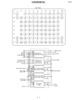
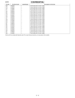
IC105 VHIYMU762C+-1L YMU762C: SOUND, Pin No., Terminal name, Input/Output, Description of terminal
 |
View all Sharp GX30 manuals
Add to My Manuals
Save this manual to your list of manuals |
Page 127 highlights
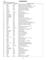
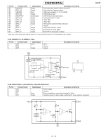
IC105 VHIYMU762C+-1L (YMU762C): SOUND Pin No. 1 2 3 4 5* 6 7 8 9 10 11 12 13 14 15 16 17 18 19 20 21 22 23 24 25 26 27 28 29 30 31 32 Terminal name CLKI LED /IRQ /RST NC PLLC VDD VSS VREF HPOUT-L/MONO HPOUT-R EQ1 EQ2 EQ3 SPVDD SPVSS SPOUT1 SPOUT2 MTR D7 D6 D5 D4 D3 D2 D1 D0 /WR /CS A0 /RD IOVDD Input/Output Input Output Output Input - - - - - Output Output - - - - - Output Output Output Input/Output Input/Output Input/Output Input/Output Input/Output Input/Output Input/Output Input/Output Input Input Input Input - CONFIDENTIAL Description of terminal Clock input terminal External LED control terminal Interrupt output terminal Hardware reset input terminal Not used Built-in PLL capacitor terminal Power supply (Typ + 3.0 V) Ground Analog reference voltage terminal Headphone output L-ch Headphone output R-ch Equalizer terminal 1 Equalizer terminal 2 Equalizer terminal 3 Analog power supply for speaker amplifier (Typ + 3.6 V) Analog ground for speaker amplifier Speaker terminal 1 Speaker terminal 2 External motor control terminal CPU I/F data bus 7 CPU I/F data bus 6 CPU I/F data bus 5 CPU I/F data bus 4 CPU I/F data bus 3 CPU I/F data bus 2 CPU I/F data bus 1 CPU I/F data bus 0 CPU I/F write enable CPU I/F chip select input CPU I/F address signal CPU I/F read enable Power supply for terminal In this unit, the terminal with asterisk mark (*) is (open) terminal which is not connected to the outside. GX30 Control register SRAM/ROM HPOUT-R HPOUT-L/ MONO IOVDD VDD VSS PLLC CLKI /RST 4 32 7 8 6 1 PLL Timing Generator /CS 29 A0 30 /WR 28 /RD 31 20 ~ 27 D0~D7 CPU interface Interface register Intermediate register FiFO 64 byte FiFO 512 byte Sequencer Buffer /IRQ 3 LED 2 MTR 19 NC 5 LED control Vibrator control TIMER Soft IRQ 11 10 HP Vol R HP Vol L FM + Wave Table Synthesizer R-ch Vol Vol L-ch R-ch 16-bit DAC L-ch Select Mono EQ 12 EQ1 Vol PCM/ADPCM Play back VREF +- SP Vol 13 EQ2 14 EQ3 VREF 9 Analog power supply for speaker amplifier 17 SPOUT1 18 SPOUT2 16 15 VREF SPVSS SPVDD 6 - 7
-
 1
1 -
2
-
3
-
4
-
5
-
6
-
7
-
8
-
9
-
10
-
11
-
12
-
13
-
14
-
15
-
16
-
17
-
18
-
19
-
20
-
21
-
22
-
23
-
24
-
25
-
26
-
27
-
28
-
29
-
30
-
31
-
32
-
33
-
34
-
35
-
36
-
37
-
38
-
39
-
40
-
41
-
42
-
43
-
44
-
45
-
46
-
47
-
48
-
49
-
50
-
51
-
52
-
53
-
54
-
55
-
56
-
57
-
58
-
59
-
60
-
61
-
62
-
63
-
64
-
65
-
66
-
67
-
68
-
69
-
70
-
71
-
72
-
73
-
74
-
75
-
76
-
77
-
78
-
79
-
80
-
81
-
82
-
83
-
84
-
85
-
86
-
87
-
88
-
89
-
90
-
91
-
92
-
93
-
94
-
95
-
96
-
97
-
98
-
99
-
100
-
101
-
102
-
103
-
104
-
105
-
106
-
107
-
108
-
109
-
110
-
111
-
112
-
113
-
114
-
115
-
116
-
117
-
118
-
119
-
120
-
121
-
 122
122 -
 123
123 -
 124
124 -
 125
125 -
 126
126 -
 127
127 -
 128
128 -
 129
129 -
 130
130 -
 131
131 -
 132
132 -
133
-
134
-
135
-
136
-
137
-
138
-
139
-
140
-
141
-
142
-
143
-
144
-
145
-
146
-
147
-
148
-
149
-
150
-
151
-
152
-
153
-
154
-
155
-
156
-
157
-
158
-
159
-
160
-
161
-
162
-
163
-
164
-
165
-
166
 |
 |
