Sony HCD-HX7 Service Manual - Page 53
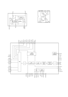
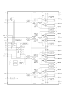
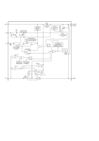
Board, Ic101 Cd-mp3 Processor, Tc94a70fg-006 Hx7,tc94a70fg-007 S, D Hx3/hx5, Pin No., Pin Name,
 |
View all Sony HCD-HX7 manuals
Add to My Manuals
Save this manual to your list of manuals |
Page 53 highlights
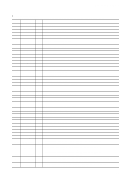
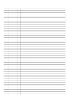
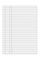
HCD-HX3/HX5/HX7 • IC Pin Function Description CD BOARD IC101 (CD-MP3 PROCESSOR) TC94A70FG-006 (HX7),TC94A70FG-007 (S, D) (HX3/HX5) Pin No. 1 2 3 4 5 6 7 8 9 10 11 12 13 14 15 16 17 18 19 20 21 22 23 24 25 26 27 28 29 30 31 32 33 34 35 36 37 Pin Name AVSS3 RFZi RFRP SBAD/RFDC FEi TEi TEZi AVDD3 FOo TRo VREF FMo DMo VSSP3 VCOi VDDP3 VDD1 VSS FGiN IO0 (/HSO) IO1 (/UHSO) XVSS3 XI XO XVDD3 DVSS3 RO DVDD3 DVR LO DVSS3 VDDT3 VSS1 VDD1 VDDM1 SRAMSTB XRST 38, 39 BUS0, BUS1 I/O Description - Ground terminal I RF ripple zero crossing signal input terminal O RF ripple signal output terminal O Sub beam addition signal or RF peak detection signal output terminal Not used O Focus error signal output terminal Not used O Tracking error signal output terminal I Tracking error zero crossing signal input terminal - Power supply terminal (+3.3 V) O Focus coil drive signal output terminal O Tracking coil drive signal output terminal I Reference voltage (+1.65V) input terminal O Sled motor drive signal output terminal O Spindle motor drive signal output terminal - Ground terminal I VCO control voltage input terminal - Power supply terminal (+3.3 V) - Power supply terminal (+1.5 V) - Ground terminal I FG signal input terminal Not used I Disc inner position detection signal input terminal O Not used - Ground terminal I System clock input terminal (16.9344 MHz) O System clock output terminal (16.9344 MHz) - Power supply terminal (+3.3 V) - Ground terminal O Audio data (R-ch) output to the input selector - Power supply terminal (+3.3 V) O Reference voltage (+1.65V) output terminal O Audio data (L-ch) output to the input selector - Ground terminal - Power supply terminal (+3.3 V) - Ground terminal - Power supply terminal (+1.5 V) - Power supply terminal (+1.5 V) I S-RAM standby mode control signal input terminal Fixed at "L" in this set I Reset signal input from the system controller "L": reset I Serial data input from the system controller and USB controller (HX3/HX5) Serial data input from the system controller (HX7) 40 BUS2 (SO) I Serial data input from the system controller and USB controller (HX3/HX5) Serial data input from the system controller (HX7) 41 BUS3 (SI) I Serial data input from the system controller and USB controller (HX3/HX5) Serial data input from the system controller (HX7) 42 BUCK (CLK) I Serial data transfer clock signal input from the system controller and USB controller (HX3/HX5) Serial data transfer clock signal input from the system controller (HX7) 43 XCCE I Chip enable signal input from the system controller and USB controller (HX3/HX5) Chip enable signal input from the system controller (HX7) 53
-
 1
1 -
2
-
3
-
4
-
5
-
6
-
7
-
8
-
9
-
10
-
11
-
12
-
13
-
14
-
15
-
16
-
17
-
18
-
19
-
20
-
21
-
22
-
23
-
24
-
25
-
26
-
27
-
28
-
29
-
30
-
31
-
32
-
33
-
34
-
35
-
36
-
37
-
38
-
39
-
40
-
41
-
42
-
43
-
44
-
45
-
46
-
47
-
 48
48 -
 49
49 -
 50
50 -
 51
51 -
 52
52 -
 53
53 -
 54
54 -
 55
55 -
 56
56 -
 57
57 -
 58
58 -
59
-
60
-
61
-
62
-
63
-
64
-
65
-
66
-
67
-
68
-
69
-
70
-
71
-
72
-
73
-
74
-
75
-
76
-
77
-
78
-
79
-
80
-
81
-
82
-
83
-
84
-
85
-
86
-
87
-
88
-
89
-
90
 |
 |