Sony STR-K7100 Service Manual - Page 48
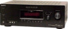
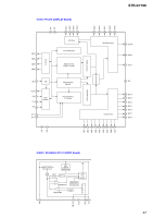
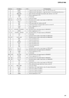
Ic1501 Cxd9718bq Digital Signal Processor Digital Board 1/3
 |
View all Sony STR-K7100 manuals
Add to My Manuals
Save this manual to your list of manuals |
Page 48 highlights
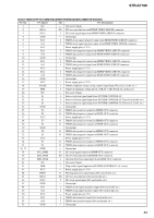
STR-K7100 • IC Pin Descriptions IC1501 CXD9718BQ (DIGITAL SIGNAL PROCESSOR) (DIGITAL BOARD (1/3)) Pin No. Pin Name I/O Pin Description 1 VSS - Ground pin 2 XRST I Reset signal input from system control IC 3 EXTIN I Not used. (Connect to ground.) 4 LRCKI3 I Not used. (Connect to ground.) 5 VDDI I Power supply pin (+1.9 V) 6 BCKI3 I Not used. (Connect to ground.) 7 PLOCK O Not used. (Open) 8 VSS - Ground pin 9 MCLK1 I Clock signal input (13.9 MHz) 10 VDDI I Power supply pin (+1.9 V) 11 VSS - Ground pin 12 MCLK2 O Clock signal output (13.9 MHz) 13 MS I Not used. (Fixed at L.) 14 SCKOUT O Internal system clock signal output for 6CH D/A converter IC 15 LRCKI1 I Sampling clock signal input from A/D converter IC 16 VDDE I Power supply pin (+3.3 V) 17 BCKI1 I Bit clock signal input from A/D converter IC 18 SDI1 I Audio IF data input from A/D converter IC 19 LRCKO O Sampling clock signal output for 6CH D/A converter IC 20 BCKO O Bit clock signal output for 6CH D/A converter IC 21 VSS - Ground pin 22 KFSIO I/O Audio clock signal (384fs/256fs) input/output for digital audio interface receiver IC 23 to 26 SDO1 to SDO4 O Digital audio serial data output for 6CH D/A converter IC 27 SPDIF O Not used. (Open) 28 LRCKI2 I Sampling clock signal input from A/D converter IC 29 BCKI2 I Bit clock signal input from A/D converter IC 30 SDI2 I Digital audio serial data input from digital audio interface receiver IC 31 VSS - Ground pin 32 HACN O Acknowledge signal output for system control IC 33 HDIN I Serial data input from system control IC 34 HCLK I Clock signal input from system control IC 35 HDOUT O Serial data output for system control IC 36 HCS I Chip select signal input from system control IC 37 GP12 I GP12 signal input from system control IC 38, 39 GP13, GP14 O Not used. (Open) 40 VDDI I Power supply pin (+1.9 V) 41 VSS - Ground pin 42 GP15 O Not used. (Open) 43 OE0 O SDRAM enable signal output 44 CS0 O External memory chip select signal output for SDRAM IC 45 WE0 O SDRAM write enable signal output for SDRAM IC 46 VDDE I Power supply pin (+3.3 V) 47 WMD1 I Not used. (Fixed at H.) 48 VSS - Ground pin 49 WMD0 I Not used. (Fixed at H.) 50 PAGE2 O Not used. (Open) 51 VSS - Ground pin 52, 53 PAGE1, PAGE0 O Not used. (Open) 54 BOOT I Not used. (Connect to ground.) 55 TST1 O Not used. (Open) 56 BST I Boot stop signal input 48
-
 1
1 -
2
-
3
-
4
-
5
-
6
-
7
-
8
-
9
-
10
-
11
-
12
-
13
-
14
-
15
-
16
-
17
-
18
-
19
-
20
-
21
-
22
-
23
-
24
-
25
-
26
-
27
-
28
-
29
-
30
-
31
-
32
-
33
-
34
-
35
-
36
-
37
-
38
-
39
-
40
-
41
-
42
-
 43
43 -
 44
44 -
 45
45 -
 46
46 -
 47
47 -
 48
48 -
 49
49 -
 50
50 -
 51
51 -
 52
52 -
 53
53 -
54
-
55
-
56
-
57
-
58
-
59
-
60
-
61
-
62
-
63
-
64
-
65
-
66
-
67
-
68
-
69
-
70
-
71
-
72
-
73
-
74
 |
 |