Compaq ProLiant 1000 Memory technology evolution: an overview of system memory - Page 14
DDR-3, Module naming convention and peak bandwidth
 |
View all Compaq ProLiant 1000 manuals
Add to My Manuals
Save this manual to your list of manuals |
Page 14 highlights
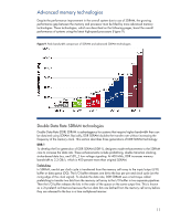
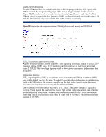
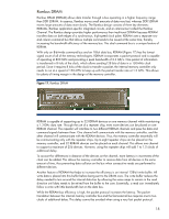
DDR-3 DDR-3, the third-generation of DDR SDRAM technology, will make further improvements in bandwidth and power consumption. Manufacturers of DDR-3 will initially use 90 nm fabrication technology and move toward 70 nm as production volumes increase. DDR-3 will operate at clock rates from 400 MHz to 800 MHz with theoretical peak bandwidths ranging from 6.40 GB/s to 12.8 GB/s. DDR-3 is expected to reduce power consumption by up to 30% compared to a DDR-2 DIMM operating at the same speed. DDR-3 DIMMs are expected to use the same 240-pin connector as DDR2 DIMMs, but the key notch will be in a different position. To increase performance and reduce power consumption of DDR-3, designers made several key enhancements, including: • An 8-bit prefetch buffer, compared to the 4-bit buffer for DDR-2, storing more data before it is needed. • Fly-by topology (for the commands, addresses, control signals, and clocks) improves signal integrity by reducing the number of stubs and their length. This feature requires the controller to support "write leveling" on DDR-3 DIMMs. • 1.5-V signaling (compared to 1.8 V for DDR-2) for lower power consumption • A thermal sensor integrated on the DIMM module signals the chipset to throttle memory traffic to the DIMM if its temperature exceeds a programmable critical trip point. Module naming convention and peak bandwidth Table 1 summarizes the various types of DDR-1, DDR-2, and DDR-3 SDRAM and their associated naming conventions. Originally, the module naming convention for DDR-SDRAM was based on the effective clock rate of the data transfer: PC200 for DDR SDRAM that operates at 100 MHz; PC266 for 133 MHz; and so forth. But after confusion arose over the Rambus naming convention, the industry based the DDR-SDRAM naming convention on the actual peak data transfer rate in MB/s. For example, PC266 is equivalent to PC2100 (64 bit * 2 * 133 MHz = 2.1 GB/s or 2100 MB/s). Table 1. Summary of DDR SDRAM technologies Type DDR-1 DDR-2 DDR-3 Component naming convention DDR200 DDR266 DDR333 DDR400 DDR2-400 DDR2-533 DDR2-667 DDR2-800 DDR3-800 DDR3-1066 DDR3-1333 DDR3-1600 Module naming convention PC1600 PC2100 PC2700 PC3200 PC2-3200R PC2-4300 PC2-5300 PC2-6400 PC3-6400 PC3-8500 PC3-10600 PC3-12800 Bus speed 100 MHz 133 MHz 166 MHz 200 MHz 200 MHz 266 MHz 333 MHz 400 MHz 400 MHz 533 MHz 667 MHz 800 MHz Peak bandwidth 1.6 GB/s 2.1 GB/s 2.7 GB/s 3.2 GB/s 3.2 GB/s 4.3 GB/s 5.3 GB/s 6.4 GB/s 6.4 GB/s 8.5 GB/s 10.6 GB/s 12.8 GB/s 14
-
 1
1 -
2
-
3
-
4
-
5
-
6
-
7
-
8
-
 9
9 -
 10
10 -
 11
11 -
 12
12 -
 13
13 -
 14
14 -
 15
15 -
 16
16 -
 17
17 -
 18
18 -
 19
19 -
20
 |
 |
