Compaq ProLiant 1000 Memory technology evolution: an overview of system memory - Page 7
Bank interleaving, Increased bandwidth, Registered SDRAM modules - parts
 |
View all Compaq ProLiant 1000 manuals
Add to My Manuals
Save this manual to your list of manuals |
Page 7 highlights
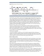
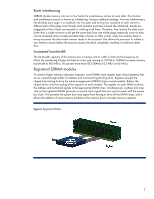
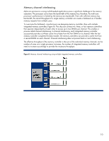
Bank interleaving SDRAM divides memory into two to four banks for simultaneous access to more data. This division and simultaneous access is known as interleaving. Using a notebook analogy, two-way interleaving is like dividing each page in a notebook into two parts and having two assistants to each retrieve a different part of the page. Even though each assistant must take a break (be refreshed), breaks are staggered so that at least one assistant is working at all times. Therefore, they retrieve the data much faster than a single assistant could get the same data from one whole page, especially since no data can be accessed when a single assistant takes a break. In other words, while one memory bank is being accessed, the other bank remains ready to be accessed. This allows the processor to initiate a new memory access before the previous access has been completed, resulting in continuous data flow. Increased bandwidth The bandwidth capacity of the memory bus increases with its width (in bits) and its frequency (in MHz). By transferring 8 bytes (64 bits) at a time and running at 100 MHz, SDRAM increases memory bandwidth to 800 MB/s, 50 percent more than EDO DRAMs (533 MB/s at 66 MHz). Registered SDRAM modules To achieve higher memory subsystem capacity, some DIMMs have register logic chips (registers) that act as a pass-through buffer for address and command signals (Figure 6). Registers prevent the chipset from having to drive the entire arrangement of DRAM chips on each module. Rather, the chipset drives only the loading of the registers on each module. The register on each DIMM re-drives the address and command signals to the appropriate DRAM chip. Simultaneously, a phase lock loop chip on the registered DIMM generates a second clock signal that runs synchronously with the system bus clock. This prevents the system bus clock signal from having to drive all the DRAM chips, and it allows the addition of more memory modules to the memory bus to increase memory capacity. Figure 6. Registered DIMMs 7
-
 1
1 -
 2
2 -
 3
3 -
 4
4 -
 5
5 -
 6
6 -
 7
7 -
 8
8 -
 9
9 -
 10
10 -
 11
11 -
 12
12 -
13
-
14
-
15
-
16
-
17
-
18
-
19
-
20
 |
 |
