Compaq ProLiant 1000 Memory technology evolution: an overview of system memory - Page 6
SDRAM technology, Clock, Command, Address
 |
View all Compaq ProLiant 1000 manuals
Add to My Manuals
Save this manual to your list of manuals |
Page 6 highlights
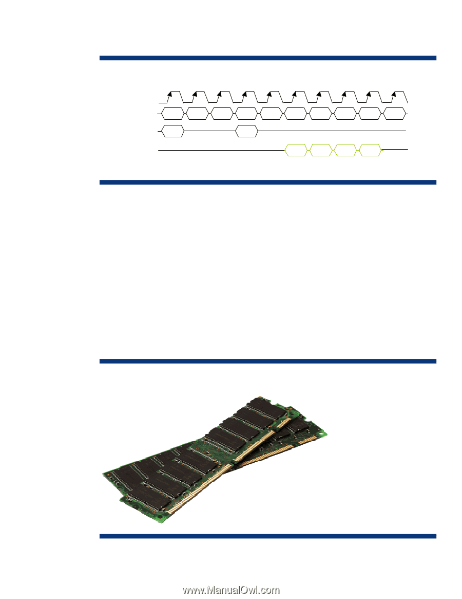
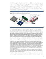
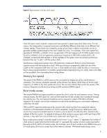
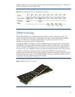
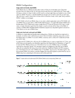
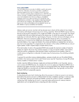
additional data sections are accessed with every clock cycle after the first access (6-1-1-1) before the memory controller has to send another CAS. Figure 4. Burst mode access. NOP is a "No Operation" instruction. Clock Command Address Data Active NOP NOP Read NOP NOP NOP NOP NOP NOP Row Col Data Data Data Data 64b 64b 64b 64b SDRAM technology FPM and EDO DRAMs are controlled asynchronously, that is, without a memory bus clock. The memory controller determined when to assert signals and when to expect data based on absolute timing. The inefficiencies of transferring data between a synchronous system bus and an asynchronous memory bus resulted in longer latency. Consequently, JEDEC-the electronics industry standards agency for memory devices and modules- developed the synchronous DRAM standard to reduce the number of system clock cycles required to read or write data. SDRAM uses a memory bus clock to synchronize the input and output signals on the memory chip. This simplified the memory controller and reduced the latency from CPU to memory. In addition to synchronous operation and burst mode access, SDRAM has other features that accelerate data retrieval and increase memory capacity-multiple memory banks, greater bandwidth, and register logic chips. Figure 5 shows SDRAM DIMMs with two key notches that prevent incorrect insertion and indicate a particular feature of the module. Figure 5. SDRAM DIMM with two notches 6
-
 1
1 -
 2
2 -
 3
3 -
 4
4 -
 5
5 -
 6
6 -
 7
7 -
 8
8 -
 9
9 -
 10
10 -
 11
11 -
 12
12 -
13
-
14
-
15
-
16
-
17
-
18
-
19
-
20
 |
 |