Epson 2180 Service Manual - Page 25
Control Circuit - diagram
 |
UPC - 010343815766
View all Epson 2180 manuals
Add to My Manuals
Save this manual to your list of manuals |
Page 25 highlights
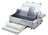
LQ-2180 Revision A 2.1 Control Circuit The control circuit of the LQ-2180 is composed of the C272MAIN board and the C165PNL board. This section describes the operations of the major components in the circuit. 2.1.1 Overview of the Control Circuit Operation The printer's control circuit includes a CPU (TMP96C141AF/IC4) that runs at 19.66 MHz, a gate array (E05B42/IC3), a 1M bit PS-RAM (IC8), a 8M bit CG-ROM (IC6), and so on. The figure below shows the block diagram for the control circuit. C N 1 ( P a r a lle l I/F ) C 1 6 5 P N L b o a rd IC 1 0 (8 M P -R O M ) IC 3 (E 0 5 B 4 2 ) CN8 T r.(Q 4 -2 5 ) CN9 D a ta A d d re s s IC 7 (n o t m o u n te d ) IC 6 (8 M C G )* 1 IC 4 (T M P 9 6 C ) IC 5 (A T 9 3 C 4 5 ) IC 8 (1 M P S -R A M ) C N 2 (T y p e B I/F ) C N 3 (fro m P S ) C N 1 4 ( S e r ia l I/F ) C N 1 7 (F a n ) C N 6 (P E -F ro n t) C N 5 (P E -R e a r) C N 7 (T o p ) C N 4 (C R H P ) IC 1 2 (A 2 9 1 7 ) C N 1 0 (P F ) IC 1 1 (S L A 7 0 2 4 M ) C N 1 1 (C R ) IC 2 (P S T 5 9 2 ) * 1 : O n ly fo r K o r e a a n d T h a i v e r s io n s C N 1 6 ( R e le a s e 2 ) C N 1 2 ( R e le a s e 1 ) C N 1 3 (P G 1 ) Figure 2-1. Control Circuit Block Diagram The following figure shows the data flow from the host computer to the printhead. Data sent from the host computer is converted to image data and transmitted to the printhead through the gate array. O p tio n I/F P a r a lle l I/F CPU TM P 96C 141 G a te A rra y E 05B 42 D a ta la tc h and d a ta o u tp u t P r in th e a d d r iv e c ir c u it P r in t d a ta c o n v e r s io n 1 P r in t d a ta c o n v e r s io n 2 Im a g e d a ta tra n s fe r Figure 2-2. Data Flow RAM In p u t B u ffe r L in e E d it B u ffe r Im a g e B u ffe r Operating Principles Control Circuit 25
-
 1
1 -
2
-
3
-
4
-
5
-
6
-
7
-
8
-
9
-
10
-
11
-
12
-
13
-
14
-
15
-
16
-
17
-
18
-
19
-
 20
20 -
 21
21 -
 22
22 -
 23
23 -
 24
24 -
 25
25 -
 26
26 -
 27
27 -
 28
28 -
 29
29 -
 30
30 -
31
-
32
-
33
-
34
-
35
-
36
-
37
-
38
-
39
-
40
-
41
-
42
-
43
-
44
-
45
-
46
-
47
-
48
-
49
-
50
-
51
-
52
-
53
-
54
-
55
-
56
 |
 |
