Intel BOXDP67BA Product Specification - Page 9

Regulatory Compliance and Battery Disposal Information, s, Tables
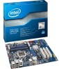
Page 9 highlights

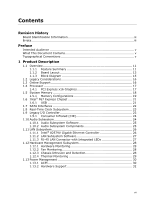
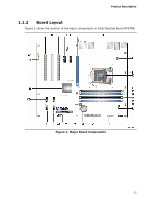
Contents 5 Regulatory Compliance and Battery Disposal Information 5.1 Regulatory Compliance 77 5.1.1 Safety Standards 77 5.1.2 European Union Declaration of Conformity Statement 78 5.1.3 Product Ecology Statements 79 5.1.4 EMC Regulations 81 5.1.5 ENERGY STAR* 5.0, e-Standby, and ErP Compliance 84 5.1.6 Regulatory Compliance Marks (Board Level 85 5.2 Battery Disposal Information 86 Figures 1. Major Board Components 13 2. Block Diagram 15 3. Memory Channel and DIMM Configuration 20 4. Back Panel Audio Connectors 25 5. LAN Connector LED Locations 27 6. Thermal Sensors and Fan Headers 29 7. Location of the Standby Power LED 36 8. Detailed System Memory Address Map 38 9. Back Panel Connectors 40 10. Component-side Connectors and Headers 41 11. Connection Diagram for Front Panel Header 47 12. Connection Diagram for Front Panel USB 2.0 Headers 49 13. Location of the Jumper Block 50 14. Board Dimensions 52 15. Localized High Temperature Zones 55 Tables 1. Feature Summary 11 2. Components Shown in Figure 1 14 3. Supported Memory Configurations 18 4. Audio Jack Support 24 5. LAN Connector LED States 27 6. Effects of Pressing the Power Switch 30 7. Power States and Targeted System Power 31 8. Wake-up Devices and Events 32 9. System Memory Map 39 10. Component-side Connectors and Headers Shown in Figure 10 42 11. IEEE 1394a Header 43 12. Front Panel Audio Header for Intel HD Audio 43 13. Front Panel Audio Header for AC '97 Audio 43 14. Front Panel USB Headers 43 15. SATA Connectors 44 16. S/PDIF Header 44 17. Chassis Intrusion Header 44 ix

  • 1
  • 2
  • 3
  • 4
  • 5
  • 6
  • 7
  • 8
  • 9
  • 10
  • 11
  • 12
  • 13
  • 14
  • 15
  • 16
  • 17
  • 18
  • 19
  • 20
  • 21
  • 22
  • 23
  • 24
  • 25
  • 26
  • 27
  • 28
  • 29
  • 30
  • 31
  • 32
  • 33
  • 34
  • 35
  • 36
  • 37
  • 38
  • 39
  • 40
  • 41
  • 42
  • 43
  • 44
  • 45
  • 46
  • 47
  • 48
  • 49
  • 50
  • 51
  • 52
  • 53
  • 54
  • 55
  • 56
  • 57
  • 58
  • 59
  • 60
  • 61
  • 62
  • 63
  • 64
  • 65
  • 66
  • 67
  • 68
  • 69
  • 70
  • 71
  • 72
  • 73
  • 74
  • 75
  • 76
  • 77
  • 78
  • 79
  • 80
  • 81
  • 82
  • 83
  • 84
  • 85
  • 86
  • 87
  • 88
  • 89
  • 90

Contents
ix
5
Regulatory Compliance and Battery Disposal Information
5.1
Regulatory Compliance
.....................................................................
77
5.1.1
Safety Standards
..................................................................
77
5.1.2
European Union Declaration of Conformity Statement
................
78
5.1.3
Product Ecology Statements
...................................................
79
5.1.4
EMC Regulations
..................................................................
81
5.1.5
ENERGY STAR* 5.0, e-Standby, and ErP Compliance
.................
84
5.1.6
Regulatory Compliance Marks (Board Level)
.............................
85
5.2
Battery Disposal Information
.............................................................
86
Figures
1.
Major Board Components
..................................................................
13
2.
Block Diagram
................................................................................
15
3.
Memory Channel and DIMM Configuration
...........................................
20
4.
Back Panel Audio Connectors
............................................................
25
5.
LAN Connector LED Locations
............................................................
27
6.
Thermal Sensors and Fan Headers
.....................................................
29
7.
Location of the Standby Power LED
....................................................
36
8.
Detailed System Memory Address Map
...............................................
38
9.
Back Panel Connectors
.....................................................................
40
10. Component-side Connectors and Headers
...........................................
41
11. Connection Diagram for Front Panel Header
........................................
47
12. Connection Diagram for Front Panel USB 2.0 Headers
...........................
49
13. Location of the Jumper Block
.............................................................
50
14. Board Dimensions
...........................................................................
52
15. Localized High Temperature Zones
.....................................................
55
Tables
1.
Feature Summary
............................................................................
11
2.
Components Shown in Figure 1
.........................................................
14
3.
Supported Memory Configurations
.....................................................
18
4.
Audio Jack Support
..........................................................................
24
5.
LAN Connector LED States
................................................................
27
6.
Effects of Pressing the Power Switch
..................................................
30
7.
Power States and Targeted System Power
...........................................
31
8.
Wake-up Devices and Events
............................................................
32
9.
System Memory Map
.......................................................................
39
10. Component-side Connectors and Headers Shown in Figure 10
................
42
11. IEEE 1394a Header
..........................................................................
43
12. Front Panel Audio Header for Intel HD Audio
........................................
43
13. Front Panel Audio Header for AC ’97 Audio
..........................................
43
14. Front Panel USB Headers
..................................................................
43
15. SATA Connectors
.............................................................................
44
16. S/PDIF Header
................................................................................
44
17. Chassis Intrusion Header
..................................................................
44