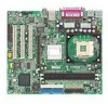
MSI 845GEM-L User Guide - Page 53
Advanced Chipset Features, Con DRAM Timing, CAS# Latency, Precharge Delay
 |
View all MSI 845GEM-L manuals
Add to My Manuals
Save this manual to your list of manuals |
Page 53 highlights
845 GM/GLM/GEM/PEM/GVM series M-ATX Mainboard Advanced Chipset Features MSI Reminds You... Change these settings only if you are familiar with the chipset. Configure DRAM Timing Selects whether DRAM timing is controlled by the SPD (Serial Presence Detect) EEPROM on the DRAM module. Setting to By SPD enables DRAM timings to be determined by BIOS based on the configurations on the SPD. Selecting Manual allows users to configure the DRAM timings manually. CAS# Latency This controls the timing delay (in clock cycles) before SDRAM starts a read command after receiving it. Settings: 1.5, 2, 2.5, 3 (clocks). 1.5 (clocks) increases the system performance the most while 3 (clocks) provides the most stable performance. Precharge Delay The field specifies the idle cycles before precharging an idle bank. Settings: 7, 6, 5 (clocks). RAS# to CAS# Delay This field allows you to set the number of cycles for a timing delay 3-12
-
 1
1 -
2
-
3
-
4
-
5
-
6
-
7
-
8
-
9
-
10
-
11
-
12
-
13
-
14
-
15
-
16
-
17
-
18
-
19
-
20
-
21
-
22
-
23
-
24
-
25
-
26
-
27
-
28
-
29
-
30
-
31
-
32
-
33
-
34
-
35
-
36
-
37
-
38
-
39
-
40
-
41
-
42
-
43
-
44
-
45
-
46
-
47
-
 48
48 -
 49
49 -
 50
50 -
 51
51 -
 52
52 -
 53
53 -
 54
54 -
 55
55 -
 56
56 -
 57
57 -
 58
58 -
59
-
60
-
61
-
62
-
63
-
64
-
65
-
66
-
67
-
68
-
69
-
70
-
71
-
72
-
73
-
74
-
75
-
76
-
77
-
78
-
79
-
80
 |
 |
