Pioneer DVL-909 Service Guide - Page 33
Srm2b256slmx70 Dvdm Assy : Ic502
 |
View all Pioneer DVL-909 manuals
Add to My Manuals
Save this manual to your list of manuals |
Page 33 highlights
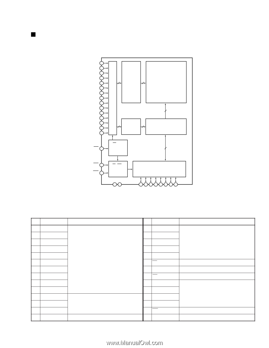
DV-505, DVL-909, DV-S9 SRM2B256SLMX70 (DVDM ASSY : IC502) • 256 K SRAM (For Mechanism Control IC) • Block Diagram A0 10 A1 9 A2 8 A3 7 A4 6 A5 5 A6 4 A7 3 A8 25 A9 24 A10 21 A11 23 A12 2 A13 26 A14 1 Address Buffer 9 Line 512 Decoder 6 Row 64 Decoder CS 20 CS Control Logic Memory-Cell Array 512×64×8 64×8 Row Gate 8 OE 22 WE 27 OE, WE Control Logic 14 18 I/O Buffer 11 12 13 15 16 17 18 19 I/O1 I/O2 I/O3 I/O4 I/O5 I/O6 I/O7 I/O8 VDD Vss • Pin Function No. Pin Name 1 A14 2 A12 3 A7 4 A6 5 A5 6 A4 7 A3 8 A2 9 A1 10 A0 11 I/O1 12 I/O2 13 I/O3 14 VSS Function Address input Data input/output GND (0V) No. Pin Name 15 I/O4 16 I/O5 17 I/O6 18 I/O7 19 I/O8 20 CS 21 A10 22 OE 23 A11 24 A9 25 A8 26 A13 27 WE 28 VDD Function Data input/output Chip select Address input Output enable Address input Write enable Power supply (2.7 to 5.5V) 33
-
 1
1 -
2
-
3
-
4
-
5
-
6
-
7
-
8
-
9
-
10
-
11
-
12
-
13
-
14
-
15
-
16
-
17
-
18
-
19
-
20
-
21
-
22
-
23
-
24
-
25
-
26
-
27
-
 28
28 -
 29
29 -
 30
30 -
 31
31 -
 32
32 -
 33
33 -
 34
34 -
 35
35 -
 36
36 -
 37
37 -
 38
38 -
39
-
40
-
41
-
42
-
43
-
44
-
45
-
46
-
47
 |
 |