Pioneer DVL-909 Service Guide - Page 43
Mb811171622a-100fn Dvdm Assy : Ic802
 |
View all Pioneer DVL-909 manuals
Add to My Manuals
Save this manual to your list of manuals |
Page 43 highlights
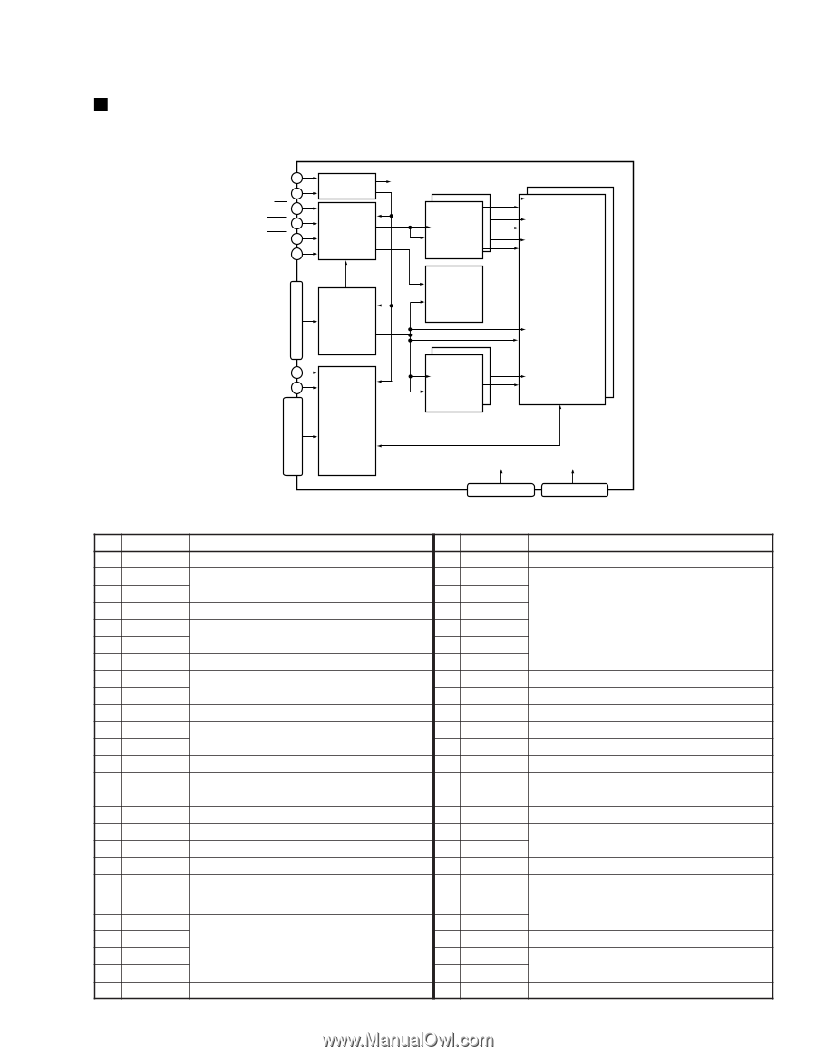
DV-505, DVL-909, DV-S9 MB811171622A-100FN (DVDM ASSY : IC802) • Code Buffer (16M bit SDRAM) • Block Diagram CLK 35 CKE 34 CS 18 RAS 17 CAS 16 WE 15 Clock Buffer Command Decoder To Blocks Control Signal Latch 21-24, 27-32, 20, 19 A0-A11, AP DQML 14 DQMU 36 DQ0-DQ15 Address Buffer/ Register & Bank Select I/O Data Buffer/ Register Mode Register Column Address Counter Bank 1 RAS Bank 0 CAS WE DRAM Core (2,048×256×16) Row Address Column Address I/O 2,3,5,6,8,9,11,12,39, 40,42,43,45,46,48,49 • Pin Function No. Pin Name 1 VCC 2 DQ0 3 DQ1 4 VSSQ 5 DQ2 6 DQ3 7 VCCQ 8 DQ4 9 DQ5 10 VSSQ 11 DQ6 12 DQ7 13 VCCQ 14 DQML 15 WE 16 CAS 17 RAS 18 CS 19 A11 (BA) 20 A10/AP 21 A0 22 A1 23 A2 24 A3 25 VCC Function Power supply (+ 3.3V) Data input/output Ground Data input/output Power supply (+ 3.3V) Data input/output Ground Data input/output Power supply (+ 3.3V) Input mask / Output enable Write enable Column address strobe Row address strobe Chip select Bank select Address input Row : A0 to A10 , Column : A0 to A7 / Auto pre-charge enable Address input Row : A0 to A10 , Column : A0 to A7 Power supply (+ 3.3V) 1,7,13,25,38,44 VCC/VCCQ 4,10,26,41,47,50 VSS/VSSQ No. Pin Name 26 VSS 27 A4 28 A5 29 A6 30 A7 31 A8 32 A9 33 DU 34 CKE 35 CLK 36 DQMU 37 DU 38 VCCQ 39 DQ8 40 DQ9 41 VSSQ 42 DQ10 43 DQ11 44 VCCQ Ground Function Address input Row : A0 to A10 , Column : A0 to A7 Don't use (use for open) Clock enable Clock input Input mask / Output enable Don't use (use for open) Power supply (+ 3.3V) Data input/output Ground Data input/output Power supply (+ 3.3V) 45 DQ12 46 DQ13 47 VSSQ 48 DQ14 49 DQ15 50 VSS Data input/output Ground Data input/output Ground 43
-
 1
1 -
2
-
3
-
4
-
5
-
6
-
7
-
8
-
9
-
10
-
11
-
12
-
13
-
14
-
15
-
16
-
17
-
18
-
19
-
20
-
21
-
22
-
23
-
24
-
25
-
26
-
27
-
28
-
29
-
30
-
31
-
32
-
33
-
34
-
35
-
36
-
37
-
 38
38 -
 39
39 -
 40
40 -
 41
41 -
 42
42 -
 43
43 -
 44
44 -
 45
45 -
 46
46 -
 47
47
 |
 |