Seagate ST3500630A Serial ATA - A Comparison with Ultra ATA Technology (57K, P - Page 3
Electrical Design Constraints - Overcoming Parallel Design Complexities with a Serial Bus - drivers
 |
UPC - 000067575145
View all Seagate ST3500630A manuals
Add to My Manuals
Save this manual to your list of manuals |
Page 3 highlights
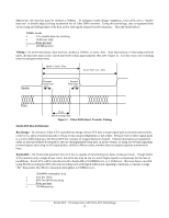
Timing - The 1.5Gbits/sec transfer rate requires bit transitions and reception to occur within 0.667ns. The maximum allowed switching time is 0.273ns, much faster than the 10ns transition time allowable for Ultra ATA. However, as seen in the following sections the electrical design parameters of the serial bus are more tightly controlled. Serial ATA can thus meet and surpass the timing required to deliver throughput comparable to that of Ultra ATA. Electrical Design Constraints - Overcoming Parallel Design Complexities with a Serial Bus Optimization of any high-speed digital bus design in fact requires careful consideration of analog design issues. Undesired analog effects associated with parallel data busses such as crosstalk, ground bounce, ringing, and clock skew have become major design constraints for the Ultra ATA interface, which is forced to maintain compatibility with legacy parallel technology. These same issues are expected to become critical roadblocks to further Ultra ATA speed increases. Serial ATA alleviates many of these problems by transitioning to a serial data bus. The intent of the following section is to first present the design methods required to achieve the current Ultra ATA data rate and illustrate the complexities of further speed enhancements to the parallel technology. In each case, the paper will describe how the Serial ATA bus architecture overcomes these complexities to extend the performance roadmap of ATA. Though full explanation of the analog design issues discussed is beyond the scope of this document, a brief overview of these noise and error sources follows to provide the reader with the background necessary to compare the electrical properties of each bus design: Ø Crosstalk results from magnetic fields generated from transitioning currents being coupled into neighboring current loops, similar to the functionality of a transformer. The magnitude of the crosstalk is proportional to the rate of the change in the current and the amount of coupling between the current loops. Thus it is most apparent in parallel busses where multiple adjacent lines may be switching in the same direction at the same time and inject a noise voltage onto a victim signal. Ø Ground bounce is most problematic when several signals switch at the same time or when using high-speed drivers, both common with parallel data busses. The instantaneous power draw is such that the decoupling capacitors for the device cannot supply the necessary current and the supply voltage sags. If the voltage decreases enough, the change can be mistaken as a bit transition. Ø Ringing results from impedance changes in a signal path in systems in which signal rise time is close to or faster than the path propagation delay. When this condition holds true, the signal path must be seen as a distributed system, implying that all points on the signal path may not be at the same voltage at the same time. As the signal propagates down a path, the voltage magnitude is related to the "effective" impedance up to the point in the signal's flight. If this impedance suddenly changes, the voltage temporarily increases to maintain the current flow. This voltage "reflects" back along the transmission line to the source, where if not fully damped may reflect again to the receiver, and may repeat until effectively damped. This causes oscillations in the voltage, or ringing, on the transmission line. Ø Clock skew results from discrepancies in transmission path delays between clock and data signals or signal degradation of the clock signal. If the clock trace is shorter than the data lines, for example, the clock signal may arrive at the receiver before the data lines have stabilized, thus registering incorrect data. Alternatively, ringing or noise on the clock line can delay the clock transition relative to the data switching, possibly violating data hold time. Electrical Design Overview Ultra ATA - Maintaining Compatibility with a Legacy Parallel Design The PC industry adopted the ATA-1 standard as the primary storage I/O interface in the mid '80s, and has maintained backward compatibility to this original standard ever since. The protocol has scaled well, from 3.3Mbytes/sec with ATA-1 to 100Mbytes/sec with ATA/ATAPI-6. However, this radical increase in speed has come with added design complexity. In the following sections, many of the key design advances to reach 100Mbyte/sec transfer rates will be discussed and their limitations for further speed increases explained. Serial ATA : A Comparison with Ultra ATA Technology - 3 -
-
 1
1 -
 2
2 -
 3
3 -
 4
4 -
 5
5 -
 6
6 -
 7
7
 |
 |
