Seagate ST3500630A Serial ATA - A Comparison with Ultra ATA Technology (57K, P - Page 4
Serial ATA - Embedded Clocking - problems
 |
UPC - 000067575145
View all Seagate ST3500630A manuals
Add to My Manuals
Save this manual to your list of manuals |
Page 4 highlights
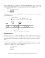
Serial ATA Electrical Design Considerations Due to the challenges in increasing the speed of the Ultra ATA specification further, a shift in design strategy is required. Serial ATA addresses this need by making the transition to a high-speed serial bus. To mitigate many of the design problems associated with high-speed single -ended and/or parallel busses, Serial ATA uses low voltage differential signaling. With this approach, each data "signal" is in fact transmitted over two lines which carry equal and opposite versions of the signal. The receiver then decodes the signal based on the differential voltage between these lines. The "common-mode" voltage, or the voltage the lines use as a DC reference plus any noise injected equally into both lines, is rejected at the receiver. This common-mode voltage may change over time, though the variations above a certain frequency may be injected into the receiver as noise. These excellent electrical properties provide many of the key design advantages that enable Serial ATA to extend beyond Ultra ATA speeds. Clocking Strategy Ultra ATA - Non-interlocked clocking Because of the high data rates and relatively high board and cable propagation delays, Ultra ATA uses non-interlocked clocking, also known as source-synchronous clocking. In typical synchronous clocking designs, data is transmitted from the source and clocked at the receiver using a local clock signal. With non-interlocked clocking, the clock or data strobe signal is generated at the source and sent with the data. Assuming identical trace or cable lengths and characteristics, both data and strobe arrive at the receiver at the same time. This technique allows more flexibility in total propagation delay along the bus, but introduces additional complexities. Because the strobe is sent with the data, it is subject to ringing and reflections. If this noise is great enough, data may be "double clocked" if the strobe signal crosses the switching threshold. Data settling time is often more critical, as the strobe transition is typically more aggressively aligned with the data transition. Clock skew becomes more complicated as well, as both data and clock propagation times may vary from the predicted delay. To reduce problems related to skew, 100MHz transfers (Ultra DMA Mode 5) must use 3.3V signaling (vs. 5V with previous ATA specs) so that signal transitions are more symmetric about the 1.5V switching threshold. Termination impedances are also more tightly constrained to reduce ringing in the signals that could cause plateaus or bumps in the signal edge, resulting in delayed threshold crossings. Serial ATA - Embedded Clocking Unlike the parallel ATA bus, Serial ATA does not have a separate signal dedicated as a strobe or clock. Instead the clock is "embedded" in the data stream itself. When no data is being sent across the bus, a "101010..." pattern is transmitted so that both devices may synchronize their internal receivers with the incoming bit transition timing. This synchronization is maintained during data transmissions. The 8b10b encoding enforces several bit transitions per 10 bits even during data transmission; clock drift is minimized by continuously tracking these transitions. Embedded clocking provides the timing benefits of source-synchronous clocking without introducing problems associated with clock skew. Cabling Ultra ATA - 80-wire ribbon cable Until ATA/ATAPI-3, or Ultra ATA 33, the ATA interface used a 40-wire cable to transmit data, of which only 7 signals were ground. Because crosstalk is proportional to the size of the mutual current loops between signal lines, the large separation between each signal and its respective return ground line results in significant crosstalk over this cable. For transfer rates greater than 33MHz (Ultra DMA Mode 3), the original 40-wire cable has been replaced by an 80-wire version with alternating ground and signal lines. This greatly minimizes crosstalk among signals and helps to balance the effective impedance of each line at high frequencies. However, the cable is specified to be at most 18" to minimize signal integrity issues. Serial ATA - 4-wire cable with support for optional shield / drain wires Serial ATA uses a minimum 4-wire cable that includes differential pairs for transmitting and receiving data. To minimize impedance and crosstalk, many cables incorporate additional shielding ground drain lines which function similarly to the 40 interspersed ground lines in the 80-pin Ultra ATA cable. The Serial ATA connector supports 3 independent ground return paths. Serial ATA cables are specified to be at max 1m in length. Serial ATA : A Comparison with Ultra ATA Technology - 4 -
-
 1
1 -
 2
2 -
 3
3 -
 4
4 -
 5
5 -
 6
6 -
 7
7
 |
 |