ASRock X99 Taichi User Manual - Page 68
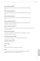
Write Recovery Time tWR, Refresh Cycle Time tRFC
 |
View all ASRock X99 Taichi manuals
Add to My Manuals
Save this manual to your list of manuals |
Page 68 highlights
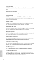
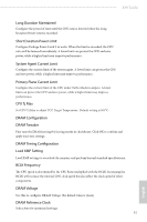
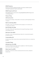
DRAM Frequency If [Auto] is selected, the motherboard will detect the memory module(s) inserted and assign the appropriate frequency automatically. DRAM Frequency OC Preset If the DRAM frequency is selected, the corresponding DRAM and BCLK frequency for overclocking will be set. Primary Timing CAS# Latency (tCL) The time between sending a column address to the memory and the beginning of the data in response. RAS# to CAS# Delay (tRCD) The number of clock cycles required between the opening of a row of memory and accessing columns within it. Row Precharge Time (tRP) The number of clock cycles required between the issuing of the precharge command and opening the next row. RAS# Active Time (tRAS) The number of clock cycles required between a bank active command and issuing the precharge command. Command Rate (CR) The delay between when a memory chip is selected and when the first active command can be issued. Secondary Timing Write Recovery Time (tWR) The amount of delay that must elapse after the completion of a valid write operation, before an active bank can be precharged. Refresh Cycle Time (tRFC) The number of clocks from a Refresh command until the first Activate command to the same rank. 62 English
-
 1
1 -
2
-
3
-
4
-
5
-
6
-
7
-
8
-
9
-
10
-
11
-
12
-
13
-
14
-
15
-
16
-
17
-
18
-
19
-
20
-
21
-
22
-
23
-
24
-
25
-
26
-
27
-
28
-
29
-
30
-
31
-
32
-
33
-
34
-
35
-
36
-
37
-
38
-
39
-
40
-
41
-
42
-
43
-
44
-
45
-
46
-
47
-
48
-
49
-
50
-
51
-
52
-
53
-
54
-
55
-
56
-
57
-
58
-
59
-
60
-
61
-
62
-
 63
63 -
 64
64 -
 65
65 -
 66
66 -
 67
67 -
 68
68 -
 69
69 -
 70
70 -
 71
71 -
 72
72 -
 73
73 -
74
-
75
-
76
-
77
-
78
-
79
-
80
-
81
-
82
-
83
-
84
-
85
-
86
-
87
-
88
-
89
-
90
-
91
-
92
-
93
-
94
-
95
-
96
-
97
-
98
 |
 |