Asus A7V400-MX SE A7V400-MX SE user's manual for English version - Page 52
DRAM Timing [Auto by SPD]
 |
View all Asus A7V400-MX SE manuals
Add to My Manuals
Save this manual to your list of manuals |
Page 52 highlights
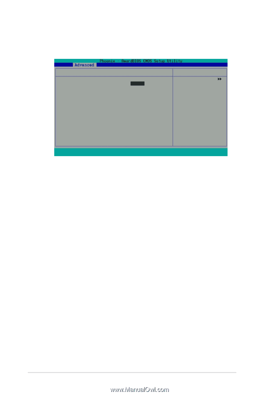
2.5.2 Memory Configuration This menu allows you to change the system memory settings. Memory Configuration Current DRAM Frequency DRAM Clock DRAM Timing DRAM CAS Latency Bank Interleave Pre-charge to Active (Trp) Active to Precharge (Tras) Active to CMD (Trcd) DRAM Burst Length DRAM Command Rate Write Recovery Time tWTR 133MHz [By SPD] [Auto by SPD] 2.5 Disabled 5T 7T 5T [4] [2T Command] [3T] [2T] Select Menu Item Specific Help Set DRAM frequency. F1 : Help ↑↓ : Select Item -/+ : Change Value F5 : Setup Defaults ESC : Exit →← : Select Menu Enter : Select Sub-menu F10 : Save and Exit Current DRAM Frequency [XXX MHz] Displays the current memory frequency as auto-detected by the BIOS. DRAM Clock [By SPD] The DRAM clock are set according to the DRAM SPD (Serial Presence Detect). You can manually set the DRAM clock parameters. Configuration options: [By SPD] [133 MHz] [166 MHz] DRAM Timing [Auto by SPD] It is recommended that you set this parameter to [Auto by SPD]. Setting to [Auto by SPD] synchronizes the DRAM timing with the DRAM clock. Setting to [Manual] allows you to set the values for DRAM CAS Latency, Bank Interleave, Pre-charge to Active (TRP) and Active to CMD (Trcd) prameters. Configuration options: [Manual] [Auto By SPD] [Safe] DRAM CAS Latency [2.5] Sets the override clock cycle for the latency time between the DRAM read command and the moment that the data actually becomes available. Normally, the system determines the rate automatically by default. Configuration options: [1.5] [2] [2.5] [3] Bank Interleave [Disabled] Sets the memory bank interleave. Configuration options: [Disabled] [2 Bank] [4 Bank] Precharge to Active (Trp) [5T] Configuration options: [2T] [3T] [4T] [5T] 2-16 Chapter 2: BIOS setup
-
 1
1 -
2
-
3
-
4
-
5
-
6
-
7
-
8
-
9
-
10
-
11
-
12
-
13
-
14
-
15
-
16
-
17
-
18
-
19
-
20
-
21
-
22
-
23
-
24
-
25
-
26
-
27
-
28
-
29
-
30
-
31
-
32
-
33
-
34
-
35
-
36
-
37
-
38
-
39
-
40
-
41
-
42
-
43
-
44
-
45
-
46
-
 47
47 -
 48
48 -
 49
49 -
 50
50 -
 51
51 -
 52
52 -
 53
53 -
 54
54 -
 55
55 -
 56
56 -
 57
57 -
58
-
59
-
60
-
61
-
62
-
63
-
64
-
65
-
66
-
67
-
68
-
69
-
70
-
71
-
72
 |
 |