Foxconn 720MX-K English Manual - Page 33
► CKE Base Power Down Mode
 |
View all Foxconn 720MX-K manuals
Add to My Manuals
Save this manual to your list of manuals |
Page 33 highlights
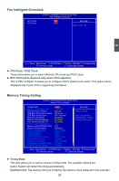
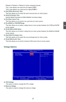
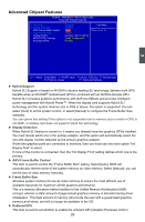
3 ► Memory Clock Value Limit This item allows you to set the system memory's clock value. ► SPD Checksum Restart The Serial Presence Detect (SPD) device is a small EEPROM chip, mounted on a DDR memory module. This item allows you to check if the memory fails when booting. Select [Ignore], the system will not check memory module. Select [Exit], system will check, report error if there is any, then stop booting. ► CKE Base Power Down Mode This item allows you to enable or disable the CKE base power down mode. ► CKE Base Power Down CKE power down mode selection. ► Memclock Tri-stating Enables the DDR memory clocks to be tristated when alternate VID mode is enabled. ► Memory Hole Remapping This item is used to enable/disable memory remapping around memory hole. PCI doesn't actually care much which addresses are used, but by convention the PC platform puts them at the top of the 32-bit address space. For many years it wasn't possible or practical to put that much RAM into a PC. But now it is, so it's up to the memory controller and host bridge to figure out what to do. Many systems cause that high RAM to simply be ignored, resulting in the loss of effective RAM. More complex systems will take the RAM that would occupy that 3.5-4GB address space and re-map it into the 4.0-4.5 address space. The RAM doesn't care because it's just an array of storage cells, it's up to the memory controller to associate addresses with those storage cells. Of course, that only works if you're using a 64-bit (or 32-bit physical address extension (PAE) enabled) OS that can deal with physical addresses larger than 32 bits. Once this option is enabled, the BIOS can see 4096MB of memory. ► Auto Optimize Bottom IO Auto optimize maximum DRAM size when kernel assigns PCI resources done. ► Bottom of [31:24] IO Space Select bottom of [31:24] IO space manually when "Auto Optimize Bottom IO" option is disabled. ► Bottom of UMA DRAM [31:24] This is a memory allocation method addition to the Unified Memory Architecture (UMA) concept. Normally, select the default value. ► Memory Timing Setting Select [Enabled], you can configure the DRAM timing manually. Select [Disabled], then system will use the DRAM timing provided by the memory vendor. The provision of DRAM timing is done by a SPD device. The Serial Presence Detect (SPD) device is a small EEPROM chip, mounted on a DDR2 memory module. It contains important information about the module's speed, size, addressing mode and various other parameters, so that the motherboard memory controller (chipset) can better access the memory device. The following 8 settings are valid only when the DRAM Timing Setting is set to [Enabled]. ► TwTr Command Delay This item allows you to select a delay time (in clock cycles) between sending the last data from a write operation to the memory and issuing a read command. ► Trfc0/1 for DIMM0/1 26
-
 1
1 -
2
-
3
-
4
-
5
-
6
-
7
-
8
-
9
-
10
-
11
-
12
-
13
-
14
-
15
-
16
-
17
-
18
-
19
-
20
-
21
-
22
-
23
-
24
-
25
-
26
-
27
-
 28
28 -
 29
29 -
 30
30 -
 31
31 -
 32
32 -
 33
33 -
 34
34 -
 35
35 -
 36
36 -
 37
37 -
 38
38 -
39
-
40
-
41
-
42
-
43
-
44
-
45
-
46
-
47
-
48
-
49
-
50
-
51
-
52
-
53
-
54
-
55
-
56
-
57
-
58
-
59
-
60
-
61
-
62
-
63
-
64
-
65
-
66
-
67
-
68
-
69
-
70
-
71
-
72
-
73
-
74
-
75
-
76
-
77
-
78
-
79
-
80
-
81
-
82
-
83
-
84
-
85
-
86
-
87
-
88
-
89
-
90
-
91
-
92
-
93
-
94
-
95
-
96
-
97
-
98
-
99
-
100
-
101
-
102
-
103
-
104
-
105
-
106
-
107
-
108
 |
 |