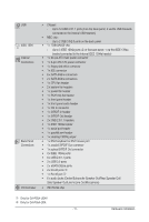
Gigabyte GA-P55A-UD4P Manual - Page 8
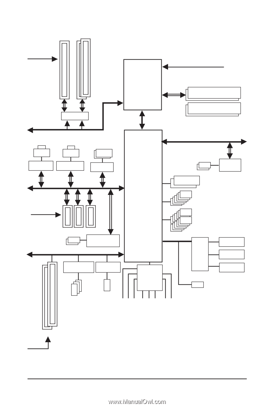
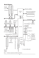
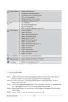
Block Diagram - ddr3
 |
UPC - 818313009081
View all Gigabyte GA-P55A-UD4P manuals
Add to My Manuals
Save this manual to your list of manuals |
Page 8 highlights
Block Diagram PCIe CLK (100 MHz) 1 PCI Express x16 or 2 PCI Express x8 x16 x8 Switch PCI Express Bus LAN LAN 2 USB 3.0/2.0 RJ45 RJ45 RTL8111D RTL8111D j x1 x1 NEC x1 PCI Express Bus x1 x1 x1 PCIe CLK (100 MHz) x1 3 PCI Express x1 2 SATA 6Gb/s PCI Bus Marvell 9128 TSB43AB23 IT8213 3 IEEE 1394a LGA1156 CPU CPU CLK+/- (133 MHz) DDR3 2200/1333/1066/800 MHz Dual Channel Memory DMI Interface PCI Express Bus x1 2 SATA 3Gb/s JMB362 Intel® P55 Dual BIOS 6 SATA 3Gb/s 12 USB 2.0/1.1 LPC Bus IT8720 Floppy COM Port CODEC PS/2 KB/Mouse TPM j(Note) ATA-133/100/66/33 IDE Channel Surround Speaker Out Center/Subwoofer Speaker Out Side Speaker Out MIC Line Out Line In S/PDIF In S/PDIF Out 2 PCI PCI CLK (33 MHz) j Only for GA-P55A-UD4P. (Note) This feature is optional due to different regional policy. - 8 -
-
 1
1 -
2
-
 3
3 -
 4
4 -
 5
5 -
 6
6 -
 7
7 -
 8
8 -
 9
9 -
 10
10 -
 11
11 -
 12
12 -
 13
13 -
14
-
15
-
16
-
17
-
18
-
19
-
20
-
21
-
22
-
23
-
24
-
25
-
26
-
27
-
28
-
29
-
30
-
31
-
32
-
33
-
34
-
35
-
36
-
37
-
38
-
39
-
40
-
41
-
42
-
43
-
44
-
45
-
46
-
47
-
48
-
49
-
50
-
51
-
52
-
53
-
54
-
55
-
56
-
57
-
58
-
59
-
60
-
61
-
62
-
63
-
64
-
65
-
66
-
67
-
68
-
69
-
70
-
71
-
72
-
73
-
74
-
75
-
76
-
77
-
78
-
79
-
80
-
81
-
82
-
83
-
84
-
85
-
86
-
87
-
88
-
89
-
90
-
91
-
92
-
93
-
94
-
95
-
96
-
97
-
98
-
99
-
100
-
101
-
102
-
103
-
104
-
105
-
106
-
107
-
108
-
109
-
110
-
111
-
112
-
113
-
114
-
115
-
116
-
117
-
118
-
119
-
120
-
121
-
122
-
123
-
124
-
125
-
126
-
127
-
128
-
129
-
130
-
131
-
132
-
133
-
134
-
135
-
136
 |
 |