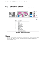
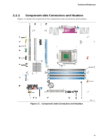
Intel DB75EN Technical Product Specification - Page 49
Table 20., Chassis Intrusion Header, Table 21., Processor, Front, and Rear Chassis, Pin Fan Headers
 |
View all Intel DB75EN manuals
Add to My Manuals
Save this manual to your list of manuals |
Page 49 highlights
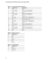
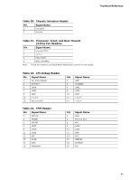
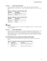
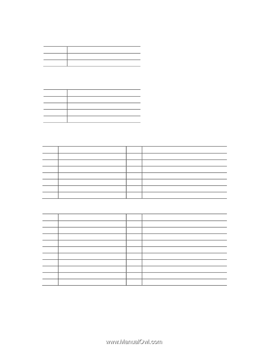
Technical Reference Table 20. Chassis Intrusion Header Pin Signal Name 1 Intruder# 2 Ground Table 21. Processor, Front, and Rear Chassis (4-Pin) Fan Headers Pin Signal Name 1 Ground (Note) 2 +12 V 3 FAN_TACH 4 FAN_CONTROL Note: These fan headers use Pulse Width Modulation control for fan speed. Table 22. LPC Debug Header Pin Signal Name 1 CK_33M_DEBUG 3 PLTRST# 5 LAD0 7 LAD2 9 GND 11 +3.3 V 13 Key (no pin) Table 23. TPM Header Pin Signal Name 1 PCICLK 3 FRAME 5 PCIRST 7 LAD3 9 VCC3 11 LAD0 13 N/C 15 3VSB 17 GND 19 PWRDWN Pin Signal Name 2 GND 4 LFRAME# 6 LAD1 8 LAD3 10 GND 12 +3.3 V 14 +3.3 V Pin Signal Name 2 GND 4 Key (no pin) 6 N/C 8 LAD2 10 LAD1 12 GND 14 N/C 16 SERIRQ 18 CLKRUN 20 N/C 49
-
 1
1 -
2
-
3
-
4
-
5
-
6
-
7
-
8
-
9
-
10
-
11
-
12
-
13
-
14
-
15
-
16
-
17
-
18
-
19
-
20
-
21
-
22
-
23
-
24
-
25
-
26
-
27
-
28
-
29
-
30
-
31
-
32
-
33
-
34
-
35
-
36
-
37
-
38
-
39
-
40
-
41
-
42
-
43
-
 44
44 -
 45
45 -
 46
46 -
 47
47 -
 48
48 -
 49
49 -
 50
50 -
 51
51 -
 52
52 -
 53
53 -
 54
54 -
55
-
56
-
57
-
58
-
59
-
60
-
61
-
62
-
63
-
64
-
65
-
66
-
67
-
68
-
69
-
70
-
71
-
72
-
73
-
74
-
75
-
76
-
77
-
78
-
79
-
80
-
81
-
82
-
83
-
84
-
85
-
86
-
87
-
88
-
89
-
90
-
91
-
92
-
93
-
94
-
95
-
96
 |
 |
Technical Reference
49
Table 20.
Chassis Intrusion Header
Pin
Signal Name
1
Intruder#
2
Ground
Table 21.
Processor, Front, and Rear Chassis
(4-Pin) Fan Headers
Pin
Signal Name
1
Ground
(Note)
2
+12 V
3
FAN_TACH
4
FAN_CONTROL
Note:
These fan headers use Pulse Width Modulation control for fan speed.
Table 22.
LPC Debug Header
Pin
Signal Name
Pin
Signal Name
1
CK_33M_DEBUG
2
GND
3
PLTRST#
4
LFRAME#
5
LAD0
6
LAD1
7
LAD2
8
LAD3
9
GND
10
GND
11
+3.3 V
12
+3.3 V
13
Key (no pin)
14
+3.3 V
Table 23.
TPM Header
Pin
Signal Name
Pin
Signal Name
1
PCICLK
2
GND
3
FRAME
4
Key (no pin)
5
PCIRST
6
N/C
7
LAD3
8
LAD2
9
VCC3
10
LAD1
11
LAD0
12
GND
13
N/C
14
N/C
15
3VSB
16
SERIRQ
17
GND
18
CLKRUN
19
PWRDWN
20
N/C