Intel E3300 Data Sheet - Page 57
Datasheet, Power/Other, BSEL1, Asynch CMOS, Output, VTT_OUT_LE, Source Synch, Input/Output, LINT0,
 |
View all Intel E3300 manuals
Add to My Manuals
Save this manual to your list of manuals |
Page 57 highlights
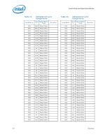
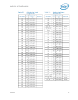
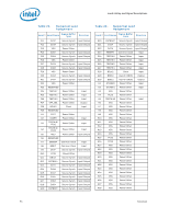
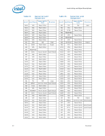
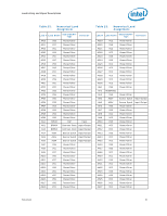
Land Listing and Signal Descriptions Table 23. Numerical Land Assignment Land # Land Name Signal Buffer Type Direction H29 FC15 Power/Other H30 BSEL1 Asynch CMOS Output J1 VTT_OUT_LE FT Power/Other Output J2 FC3 Power/Other J3 FC22 Power/Other J4 VSS Power/Other J5 REQ1# Source Synch Input/Output J6 REQ4# Source Synch Input/Output J7 VSS Power/Other J8 VCC Power/Other J9 VCC Power/Other J10 VCC Power/Other J11 VCC Power/Other J12 VCC Power/Other J13 VCC Power/Other J14 VCC Power/Other J15 VCC Power/Other J16 FC31 Power/Other J17 FC34 Power/Other J18 VCC Power/Other J19 VCC Power/Other J20 VCC Power/Other J21 VCC Power/Other J22 VCC Power/Other J23 VCC Power/Other J24 VCC Power/Other J25 VCC Power/Other J26 VCC Power/Other J27 VCC Power/Other J28 VCC Power/Other J29 VCC Power/Other J30 VCC Power/Other K1 LINT0 Asynch CMOS Input K2 VSS Power/Other K3 A20M# Asynch CMOS Input K4 REQ0# Source Synch Input/Output K5 VSS Power/Other K6 REQ3# Source Synch Input/Output K7 VSS Power/Other Table 23. Numerical Land Assignment Land # Land Name Signal Buffer Type Direction K8 K23 K24 K25 K26 K27 K28 K29 K30 L1 L2 L3 L4 L5 L6 L7 L8 L23 L24 L25 L26 L27 L28 L29 L30 M1 M2 M3 M4 M5 M6 M7 M8 M23 M24 M25 M26 M27 M28 VCC VCC VCC VCC VCC VCC VCC VCC VCC LINT1 SLP# VSS A06# A03# VSS VSS VCC VSS VSS VSS VSS VSS VSS VSS VSS VSS THERMTRIP # STPCLK# A07# A05# REQ2# VSS VCC VCC VCC VCC VCC VCC VCC Power/Other Power/Other Power/Other Power/Other Power/Other Power/Other Power/Other Power/Other Power/Other Asynch CMOS Input Asynch CMOS Input Power/Other Source Synch Input/Output Source Synch Input/Output Power/Other Power/Other Power/Other Power/Other Power/Other Power/Other Power/Other Power/Other Power/Other Power/Other Power/Other Power/Other Asynch CMOS Output Asynch CMOS Input Source Synch Input/Output Source Synch Input/Output Source Synch Input/Output Power/Other Power/Other Power/Other Power/Other Power/Other Power/Other Power/Other Power/Other Datasheet 57
-
 1
1 -
2
-
3
-
4
-
5
-
6
-
7
-
8
-
9
-
10
-
11
-
12
-
13
-
14
-
15
-
16
-
17
-
18
-
19
-
20
-
21
-
22
-
23
-
24
-
25
-
26
-
27
-
28
-
29
-
30
-
31
-
32
-
33
-
34
-
35
-
36
-
37
-
38
-
39
-
40
-
41
-
42
-
43
-
44
-
45
-
46
-
47
-
48
-
49
-
50
-
51
-
 52
52 -
 53
53 -
 54
54 -
 55
55 -
 56
56 -
 57
57 -
 58
58 -
 59
59 -
 60
60 -
 61
61 -
 62
62 -
63
-
64
-
65
-
66
-
67
-
68
-
69
-
70
-
71
-
72
-
73
-
74
-
75
-
76
-
77
-
78
-
79
-
80
-
81
-
82
-
83
-
84
-
85
-
86
-
87
-
88
-
89
-
90
-
91
-
92
-
93
-
94
-
95
-
96
-
97
-
98
-
99
-
100
 |
 |
