Lantronix XPort XPort - Integration Guide - Page 12
Recommended PCB Layout, Description and Specifications, XPort Integration Guide
 |
View all Lantronix XPort manuals
Add to My Manuals
Save this manual to your list of manuals |
Page 12 highlights
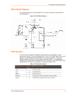
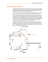
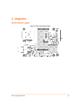
2: Description and Specifications Recommended PCB Layout The hole pattern and mounting dimensions for the XPort device server are shown in the following drawing. For proper heat dissipation, it is recommended that the PCB have approximately 1 square inch of copper attached to the shield tabs. The shield tabs are an important source of heat sinking for the device. The XPort shield is considered "chassis ground" and should be separate from "signal ground". ESD near the XPort at the panel opening will likely jump to the shield. We recommend using high voltage (~200V), low ESR, 0.01uF capacitors to connect chassis ground to both signal ground and 3.3V. This will cause any voltage spike from ESD to be imparted equally to both signal ground and 3.3V with no net voltage increase between 3.3V and signal ground. For the highest level of ESD protection of the XPort, it is recommended that the shield not be directly connected to signal GND. The metal shield fingers around the XPort's RJ45 should physically contact the product housing when the housing is metal, or metallic coated. The shield is also a heat sink for the internal EX Processor. As in all heat sinking applications, the more copper connected to the heat sink the better. Adding 1 inch square inch of copper flood on the PCB is adequate to allow the XPort to work up to +85°C. If the application does not expect to see temperatures up to +85°C the heat sink may be smaller than 1 square inch. Figure 2-7 PCB Layout XPort Integration Guide 12
-
 1
1 -
2
-
3
-
4
-
5
-
6
-
 7
7 -
 8
8 -
 9
9 -
 10
10 -
 11
11 -
 12
12 -
 13
13 -
 14
14 -
 15
15 -
 16
16 -
 17
17 -
18
 |
 |
