Lenovo PC 300PL Technical Information Manual for IBM PC300GL (Type 6563, 6564, - Page 40
Appendix A. Connector pin assignments, SVGA monitor connector
 |
View all Lenovo PC 300PL manuals
Add to My Manuals
Save this manual to your list of manuals |
Page 40 highlights
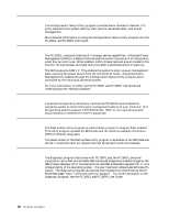
Appendix A. Connector pin assignments The following figures show the pin assignments for various system board connectors. SVGA monitor connector 5 10 15 1 6 11 Table 17. SVGA monitor port connector pin assignments Pin Signal I/O Pin 1 Red O 9 2 Green O 10 3 Blue O 11 4 Monitor ID 2 - I 12 Not used 5 Ground NA 13 6 Red ground NA 14 7 Green ground NA 15 8 Blue ground NA Signal I/O +5 V, used by NA DDC2B Ground NA Monitor ID 0 - I Not used DDC2B serial I/O data Horizontal O sync Vertical sync O DDC2B clock I/O © Copyright IBM Corp. 2000 33
-
 1
1 -
2
-
3
-
4
-
5
-
6
-
7
-
8
-
9
-
10
-
11
-
12
-
13
-
14
-
15
-
16
-
17
-
18
-
19
-
20
-
21
-
22
-
23
-
24
-
25
-
26
-
27
-
28
-
29
-
30
-
31
-
32
-
33
-
34
-
 35
35 -
 36
36 -
 37
37 -
 38
38 -
 39
39 -
 40
40 -
 41
41 -
 42
42 -
 43
43 -
 44
44 -
 45
45 -
46
-
47
-
48
-
49
-
50
-
51
-
52
-
53
-
54
-
55
-
56
-
57
-
58
-
59
-
60
-
61
-
62
-
63
-
64
-
65
-
66
-
67
-
68
-
69
 |
 |

© Copyright IBM Corp.
2000
33
Appendix A.
Connector pin assignments
The following figures show the pin assignments for various system board connectors.
SVGA monitor connector
Table 17.
SVGA monitor port connector pin assignments
Pin
Signal
I/O
Pin
Signal
I/O
1
Red
O
9
+5 V, used by
DDC2B
NA
2
Green
O
10
Ground
NA
3
Blue
O
11
Monitor ID 0 -
Not used
I
4
Monitor ID 2 -
Not used
I
12
DDC2B serial
data
I/O
5
Ground
NA
13
Horizontal
sync
O
6
Red ground
NA
14
Vertical sync
O
7
Green ground
NA
15
DDC2B clock
I/O
8
Blue ground
NA
5
1
10
6
15
11