Nintendo NES-001 User Guide - Page 16
Picture Processing Unit - store
 |
View all Nintendo NES-001 manuals
Add to My Manuals
Save this manual to your list of manuals |
Page 16 highlights
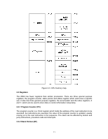
3 - Picture Processing Unit 3.1 2C02 Overview Ricoh also supplied the 2C02 to serve as PPU. The PPU's registers are mostly located in the I/O registers section of CPU memory at $2000-$2007 and $4014 as described in Appendix B. In addition, there are some special registers used for screen scrolling. 3.2 PPU Memory Map The PPU has its own memory, known as VRAM (Video RAM). Like the CPU, the PPU can also address 64 KB of memory although it only has 16 KB of physical RAM. The PPU's memory map is shown in figure 3-1. Again, the left hand map shows a simplified version which is elaborated on by the right hand map. Due to the difference between physical and logical address spaces, any address above $3FFF is wrapped around, making the logical memory locations $4000-$FFFF effectively a mirror of locations $0000-$3FFF. Reading from and writing to PPU memory can be done by using the I/O registers $2006 and $2007 in CPU memory. This is usually done during V-Blank at the end of a frame, as it affects addresses used while drawing the screen and can therefore corrupt what is displayed. However, this effect can be used to produce split screen effects. Since PPU memory uses 16-bit addresses but I/O registers are only 8-bit, two writes to $2006 are required to set the address required. Data can then be read from or written to $2007. After each write to $2007, the address is incremented by either 1 or 32 as dictated by bit 2 of $2000. The first read from $2007 is invalid and the data will actually be buffered and returned on the next read. This does not apply to colour palettes. The PPU also has a separate 256 byte area of memory, SPR-RAM (Sprite RAM), to store the sprite attributes. The sprites themselves can be found in the pattern tables. 16
-
 1
1 -
2
-
3
-
4
-
5
-
6
-
7
-
8
-
9
-
10
-
 11
11 -
 12
12 -
 13
13 -
 14
14 -
 15
15 -
 16
16 -
 17
17 -
 18
18 -
 19
19 -
 20
20 -
 21
21 -
22
-
23
-
24
-
25
-
26
-
27
-
28
-
29
-
30
-
31
-
32
-
33
-
34
-
35
-
36
-
37
-
38
-
39
-
40
-
41
-
42
-
43
-
44
-
45
-
46
-
47
 |
 |
