Nintendo NES-001 User Guide - Page 9
Central Processing Unit - controller
 |
View all Nintendo NES-001 manuals
Add to My Manuals
Save this manual to your list of manuals |
Page 9 highlights
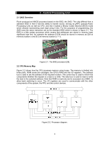
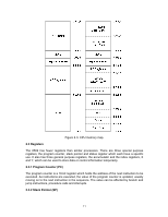
2 - Central Processing Unit 2.1 2A03 Overview Ricoh produced an NMOS processor based on the 6502, the 2A03. The chip differed from a standard 6502 in that it had the ability to handle sound, serving as pAPU (pseudo-Audio Processing Unit) as well as CPU, and that it lacked a Binary Coded Decimal (BCD) mode which allowed representing each digit using 4 bits. For the purposes of programming, the 2A03 uses the same instruction set as the standard 6502 which is shown in figure 2-1. The 6502 is a little endian processor which means that addresses are stored in memory least significant byte first, for example the address $1234 would be stored in memory as $34 at memory location x and $12 at memory location (x + 1). Figure 2-1. The 6502 processor [28]. 2.2 CPU Memory Map Figure 2-2 shows how the CPU accesses memory using buses. The memory is divided into three parts, ROM inside the cartridges, the CPU's RAM and the I/O registers. The address bus is used to set the address of the required location. The control bus is used to inform the components whether the request is a read or a write. The data bus is used to read or write the byte to the selected address. Note that ROM is read-only and is accessed via a MMC, to allow bank switching to occur. The I/O registers are used to communicate with the other components of the system, the PPU and the control devices. Figure 2-2. Processor diagram. 9
-
 1
1 -
2
-
3
-
 4
4 -
 5
5 -
 6
6 -
 7
7 -
 8
8 -
 9
9 -
 10
10 -
 11
11 -
 12
12 -
 13
13 -
 14
14 -
15
-
16
-
17
-
18
-
19
-
20
-
21
-
22
-
23
-
24
-
25
-
26
-
27
-
28
-
29
-
30
-
31
-
32
-
33
-
34
-
35
-
36
-
37
-
38
-
39
-
40
-
41
-
42
-
43
-
44
-
45
-
46
-
47
 |
 |
