Pioneer VSX-816-S Service Manual - Page 125
Pioneer VSX-816-S Manual
 |
View all Pioneer VSX-816-S manuals
Add to My Manuals
Save this manual to your list of manuals |
Page 125 highlights
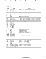
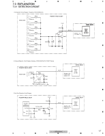
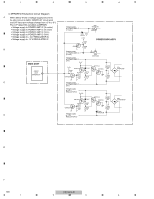
5 6 7 No. Pin Name I/O Pin Function 51 USB_DP/GPIO_B26 I/O USB function D+ signal / GPIO_B[26] 52 USB_DN/GPIO_B27 I/O USB function D- signal / GPIO_B[27] 53 USBH_DP/GPIO_B28 I/O USB host D+ signal / GPIO_B[28] 54 USBH_DN/GPIO_B29 55 VSSI 56 SD_CKE/GPIO_B0 I/O USB host D- signal / GPIO_B[29] − Digital ground for internal I/O SDRAM clock enable signal, active high / GPIO_B[0] 57 ND_nWE/GPIO_B7 I/O NAND flash WE, active low / GPIO_B[7] 58 nWE I/O Static memory write enable signal, active low 59 nOE I/O Static memory output enable signal, active low 60 UT_TX/GPIO_B8 I/O UART or IrDA TX data / GPIO_B[8] 61 UT_RX/IDE_nCS1/GPIO_B9 I/O UART or IrDA RX data / IDE chip select 1 / GPIO_B[9] 62 BCLK/GPIO_B21 I/O I2S bit clock / GPIO_B[21] 63 LRCK/GPIO_B22 64 VDD_USB 65 VSSIO I/O I2S word clock / GPIO_B[22] − Power supply for USB I/O (3.3 V) − Digital ground for I/O 66 MCLK/GPIO_B23 I/O I2S system clock / GPIO_B[23] 67 DAO/GPIO_B24 68 DAI/GPIO_B25 I/O I2S digital audio data output / GPIO_B[24] I/O I2S digital audio data input / GPIO_B[25] 69 XTIN I Sub crystal oscillator input (32.768 kHz) 70 XTOUT 71 VDD_OSC O Sub crystal oscillator output (32.768 kHz) − Digital power supply for oscillators (1.8 V) 72 nRESET I System reset, active low 73 READY I Ready information from external device 74 XIN I Main crystal oscillator input for PLL (12 MHz) 75 XOUT 76 VDDIO 77 VDDA_PLL 78 XFILT 79 VSSA_PLL 80 VBBA_PLL 81 VDDA_ADC O Main crystal oscillator output for PLL (12 MHz) − Digital power supply for I/O (1.8 V to 3.3 V) − Analog and digital power supply for PLL (1.8 V) AO PLL filter output − Analog ground for PLL − Analog ground for PLL − Analog power supply for ADC (3.3 V) 82 ADIN0 AI General purpose multi-channel ADC input 0 83 ADIN2 84 ADIN4 AI General purpose multi-channel ADC input 2 AI General purpose multi-channel ADC input 4 85 VSSA_ADC 86 VBBA_ADC − Analog ground for ADC − Analog ground for ADC 87 VDDI_ADC − Digital power supply for ADC (1.8 V) 88 VSSI_ADC 89 PKG1 − Digital ground for ADC I Package ID 1, pull-up for normal operation 90 GPIO_D15 I/O GPIO_D[15] 91 GPIO_D16 I/O GPIO_D[16] 92 GPIO_D17 I/O GPIO_D[17] 93 GPIO_D18 94 GPIO_D19 95 GPIO_D20 I/O GPIO_D[18] I/O GPIO_D[19] I/O GPIO_D[20] 96 GPIO_D21 97 VSSIO I/O GPIO_D[21] − Digital ground for I/O 98 MODE1 I Mode select input 1, Pull-down for normal operation. 99 TDI I JTAG serial data input for ARM940T 100 TMS I JTAG test mode select for ARM940T VSX-816-K 5 6 7 8 A B C D E F 125 8
-
 1
1 -
2
-
3
-
4
-
5
-
6
-
7
-
8
-
9
-
10
-
11
-
12
-
13
-
14
-
15
-
16
-
17
-
18
-
19
-
20
-
21
-
22
-
23
-
24
-
25
-
26
-
27
-
28
-
29
-
30
-
31
-
32
-
33
-
34
-
35
-
36
-
37
-
38
-
39
-
40
-
41
-
42
-
43
-
44
-
45
-
46
-
47
-
48
-
49
-
50
-
51
-
52
-
53
-
54
-
55
-
56
-
57
-
58
-
59
-
60
-
61
-
62
-
63
-
64
-
65
-
66
-
67
-
68
-
69
-
70
-
71
-
72
-
73
-
74
-
75
-
76
-
77
-
78
-
79
-
80
-
81
-
82
-
83
-
84
-
85
-
86
-
87
-
88
-
89
-
90
-
91
-
92
-
93
-
94
-
95
-
96
-
97
-
98
-
99
-
100
-
101
-
102
-
103
-
104
-
105
-
106
-
107
-
108
-
109
-
110
-
111
-
112
-
113
-
114
-
115
-
116
-
117
-
118
-
119
-
 120
120 -
 121
121 -
 122
122 -
 123
123 -
 124
124 -
 125
125 -
 126
126 -
 127
127 -
 128
128 -
 129
129 -
 130
130 -
131
-
132
-
133
-
134
-
135
-
136
-
137
-
138
-
139
-
140
-
141
-
142
-
143
-
144
 |
 |