Samsung RB195BSSB Service Manual - Page 51
Display Driving Circuit
 |
View all Samsung RB195BSSB manuals
Add to My Manuals
Save this manual to your list of manuals |
Page 51 highlights
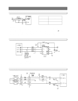
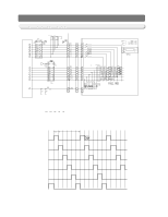
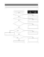
OPERATION PRINCIPLES BY PARTS OF CIRCUIT 12-8) DISPLAY DRIVING CIRCUIT 1) KEY SCAN &DISPLAY DRIVING PRINCIPLE As shown in the wave diagram below,Micom sends out "high "signals through the MICOM 6 terminals of NO #1→2→3→4→5→6 for 2ms each every 12ms.This signal goes to output terminal via input terminal of IC51 (TD62783AP or KID65783AP). Here, the peak to peak voltage of the square wave is 11~12V DC and each output wave is as follows. 2msec V 10msec GRID #1 GRID #2 GRID #3 GRID #4 GRID #5 GRID #6 T 51
-
 1
1 -
2
-
3
-
4
-
5
-
6
-
7
-
8
-
9
-
10
-
11
-
12
-
13
-
14
-
15
-
16
-
17
-
18
-
19
-
20
-
21
-
22
-
23
-
24
-
25
-
26
-
27
-
28
-
29
-
30
-
31
-
32
-
33
-
34
-
35
-
36
-
37
-
38
-
39
-
40
-
41
-
42
-
43
-
44
-
45
-
 46
46 -
 47
47 -
 48
48 -
 49
49 -
 50
50 -
 51
51 -
 52
52 -
 53
53 -
 54
54 -
 55
55 -
 56
56 -
57
-
58
-
59
-
60
-
61
-
62
-
63
-
64
-
65
-
66
-
67
-
68
-
69
-
70
-
71
-
72
-
73
-
74
-
75
-
76
-
77
-
78
-
79
-
80
 |
 |

51
OPERATION PRINCIPLES BY PARTS OF CIRCUIT
12-8) DISPLAY DRIVING CIRCUIT
GRID #1
V
T
GRID #2
GRID #3
GRID #4
GRID #5
GRID #6
2msec
10msec
1) KEY SCAN &DISPLAY DRIVING PRINCIPLE
As shown in the wave diagram below,Micom sends out “high ”signals through the MICOM 6
terminals of NO #1
→
2
→
3
→
4
→
5
→
6 for 2ms each every 12ms.This signal goes to output terminal
via input terminal of IC51 (TD62783AP or KID65783AP). Here, the peak to peak voltage of the
square wave is 11~12V DC and each output wave is as follows.