Sony HCD-HPX7 Service Manual - Page 58
Note For Printed Wiring Boards And Schematic Diagrams
 |
View all Sony HCD-HPX7 manuals
Add to My Manuals
Save this manual to your list of manuals |
Page 58 highlights
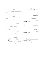
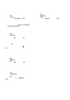
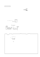
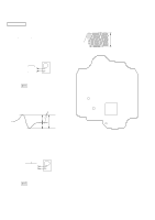
HCD-HPX7 NOTE FOR PRINTED WIRING BOARDS AND SCHEMATIC DIAGRAMS Note on Printed Wiring Boards: • X : parts extracted from the component side. • Y : parts extracted from the conductor side. • W : indicates side identified with part number. • f : internal component. • : Pattern from the side which enables seeing. (The other layers' patterns are not indicated.) Caution: Pattern face side: Parts on the pattern face side seen from (Conductor Side) the pattern face are indicated. Parts face side: Parts on the parts face side seen from (Component Side) the parts face are indicated. • Indication of transistor. C Q These are omitted. BE Q BCE These are omitted. • Waveforms - CD Board - 1 IC101 yd (LRCK) 3 IC101 uj (XTAO) 4.4 Vp-p 4.5 Vp-p Note on Schematic Diagram: • All capacitors are in µF unless otherwise noted. (p: pF) 50 WV or less are not indicated except for electrolytics and tantalums. • All resistors are in Ω and 1/4 W or less unless otherwise specified. • f : internal component. • 2 : nonflammable resistor. • 5 : fusible resistor. • C : panel designation. Note: The components identified by mark 0 or dotted line with mark 0 are critical for safety. Replace only with part number specified. • A : B+ Line. • B : B- Line. • Voltages and waveforms are dc with respect to ground un- der no-signal conditions. • Voltages are taken with a VOM (Input impedance 10 MΩ). Voltage variations may be noted due to normal production tolerances. • Waveforms are taken with a oscilloscope. Voltage variations may be noted due to normal production tolerances. • Circled numbers refer to waveforms. • Signal path. F : TUNER (FM/AM) E : TAPE PLAY a : TAPE REC J : CD PLAY L : AUX IN • Abbreviation AUS : Australian model CND : Canadian model E3 : 240 V AC area in E model KR : Korean model MX : Mexican model TW : Taiwan model - MAIN Board - 1 Q303, 304 (Collector) 4 IC306 qd (XOUT) (REC Mode) 12.4 Vp-p 2 Vp-p 22.8 µs 2 IC101 yh (BCK) 59 ns 4 IC101 ra (PFACO) 4.5 Vp-p 472 ns Approx. 700 mVp-p 21.2 µs 2 Q303, 304 (Base) (REC Mode) 62.6 ns 5 IC306 of (TC END SW) (Tape Play Mode) 2.6 Vp-p 6.3 Vp-p 21.2 µs 2 s 3 IC306 qa (XCOUT) 30.4 µs 3.2 Vp-p 58
-
 1
1 -
2
-
3
-
4
-
5
-
6
-
7
-
8
-
9
-
10
-
11
-
12
-
13
-
14
-
15
-
16
-
17
-
18
-
19
-
20
-
21
-
22
-
23
-
24
-
25
-
26
-
27
-
28
-
29
-
30
-
31
-
32
-
33
-
34
-
35
-
36
-
37
-
38
-
39
-
40
-
41
-
42
-
43
-
44
-
45
-
46
-
47
-
48
-
49
-
50
-
51
-
52
-
 53
53 -
 54
54 -
 55
55 -
 56
56 -
 57
57 -
 58
58 -
 59
59 -
 60
60 -
 61
61 -
 62
62 -
 63
63 -
64
-
65
-
66
-
67
-
68
-
69
-
70
-
71
-
72
-
73
-
74
-
75
-
76
-
77
-
78
-
79
-
80
-
81
-
82
-
83
-
84
-
85
-
86
-
87
-
88
-
89
-
90
-
91
-
92
-
93
-
94
-
95
-
96
-
97
-
98
-
99
-
100
-
101
-
102
-
103
-
104
-
105
-
106
-
107
-
108
-
109
-
110
 |
 |
