Sony STR-K790 Service Manual - Page 13
Str-k790, Diagrams - boards
 |
View all Sony STR-K790 manuals
Add to My Manuals
Save this manual to your list of manuals |
Page 13 highlights
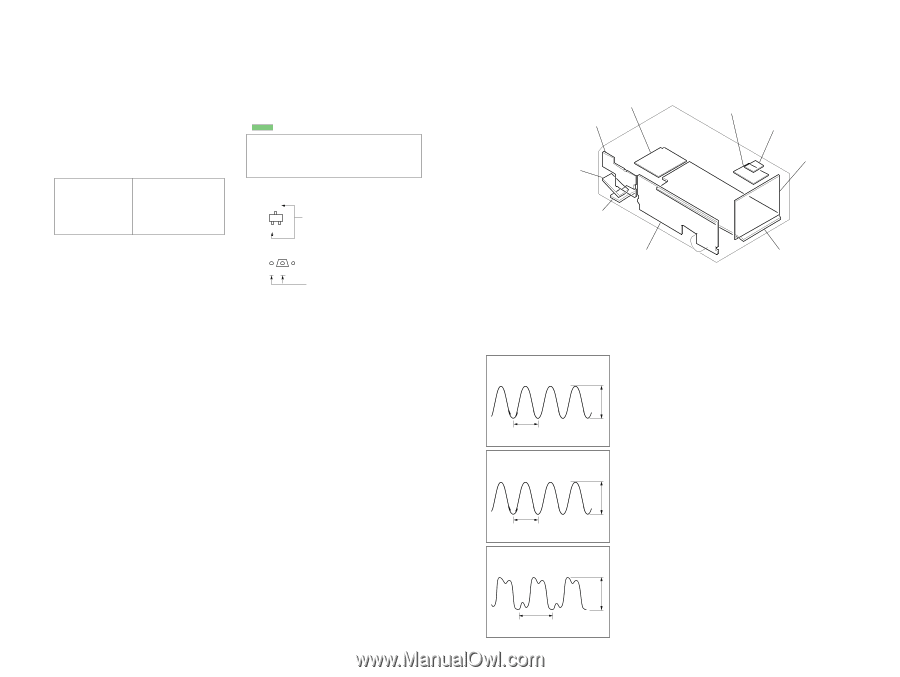
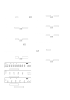
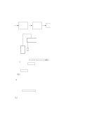
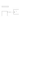
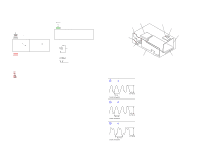
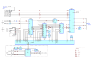
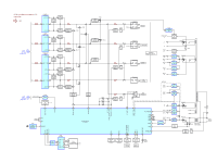
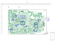
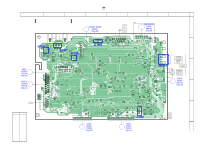
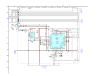
SECTION 4 DIAGRAMS THIS NOTE IS COMMON FOR PRINTED WIRING BOARDS AND SCHEMATIC DIAGRAMS. (In addition to this, the necessary note is printed in each block.) For Schematic Diagrams. Note: • All capacitors are in µF unless otherwise noted. (p: pF) 50 WV or less are not indicated except for electrolytics and tantalums. • All resistors are in Ω and 1/4 W or less unless otherwise specified. • % : indicates tolerance. • f : internal component. • 2 : nonflammable resistor. • 5 : fusible resistor. • C : panel designation. Note: The components identified by mark 0 or dotted line with mark 0 are critical for safety. Replace only with part number specified. Note: Les composants identifiés par une marque 0 sont critiques pour la sécurité. Ne les remplacer que par une piéce portant le numéro spécifié. • A : B+ Line. • B : B- Line. • Voltages and waveforms are dc with respect to ground un- der no-signal (detuned) conditions. No mark : FM • Voltages are taken with a VOM (Input impedance 10 MΩ). Voltage variations may be noted due to normal production tolerances. • Waveforms are taken with a oscilloscope. • Circled numbers refer to waveforms. • Signal path. F : FM J : ANALOG c : DIGITAL I : VIDEO For Printed Wiring Boards. Note: • X : parts extracted from the component side. • a : Through hole. • f : internal component. • : Pattern from the side which enables seeing. Caution: Pattern face side: (Side B) Parts face side: (Side A) Parts on the pattern face side seen from the pattern face are indicated. Parts on the parts face side seen from the parts face are indicated. • Indication of transistor. C Q These are omitted. BE BCE These are omitted. • Circuit Boards Location STANDBY board POWER board DCAC board HEADPHONE board DISPLAY board STR-K790 HDMI SW board (AEP,UK) HDMI BRIDGE board (AEP,UK) DIGITAL board MAIN board • Waveforms - DIGITAL Board - 1 IC1905 9 (MCLK1) 72 ns 1 V/DIV, 40 ns/DIV 2 IC1101 id (X1) 3.5 Vp-p 41.6 ns 1 V/DIV, 20 ns/DIV 3 IC1301 ws (XIN) 4.2 Vp-p STR-K790 81.4 ns 1 V/DIV, 40 ns/DIV 4.2 Vp-p 13 13
-
 1
1 -
2
-
3
-
4
-
5
-
6
-
7
-
 8
8 -
 9
9 -
 10
10 -
 11
11 -
 12
12 -
 13
13 -
 14
14 -
 15
15 -
 16
16 -
 17
17 -
 18
18 -
19
-
20
-
21
-
22
-
23
-
24
-
25
-
26
-
27
-
28
-
29
-
30
-
31
-
32
-
33
-
34
-
35
-
36
-
37
-
38
-
39
-
40
-
41
-
42
-
43
-
44
-
45
-
46
-
47
-
48
-
49
-
50
-
51
-
52
-
53
-
54
-
55
-
56
 |
 |