HP ProLiant DL380p DDR3 memory technology - Page 6
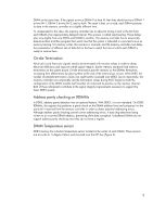
On-die Termination, Address parity checking on RDIMMs, DIMM Temperature sensor
 |
View all HP ProLiant DL380p manuals
Add to My Manuals
Save this manual to your list of manuals |
Page 6 highlights
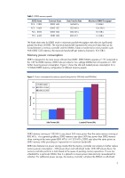
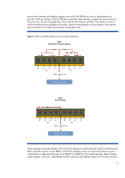
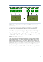
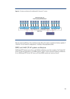
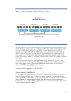
DRAM at the same time. If the signals arrive at DRAM 0 at time N, then they should arrive at DRAM 1 at time N+1, DRAM 2 at time N+2, and so forth. The result is that, on a read, each DRAM presents its data to the memory controller at a slightly different time. To compensate for this skew, the memory controller has to adjust its timing to lock in the bits from each DRAM at an appropriately delayed interval. This process is called read leveling. These delays also vary slightly from one DRAM and DIMM to another. The memory controller has to empirically determine them and then program them each time that the system is rebooted in a process known as memory training. For memory writes, this scenario is reversed, and the memory controller must delay the presentation of different sets of data bits to the bus to match the time at which each DRAM is ready to receive them. On-die Termination Electrical circuits that carry signals need to be terminated with resistive values in order to damp electrical reflections and improve overall signal integrity. Earlier memory standards had memory termination on the system board. On-die termination puts the resistors on the DRAMs themselves, increasing their effectiveness by placing them at the end of the memory bus circuits. With DDR3, the number of possible termination values was significantly increased over DDR2. Just as importantly, the memory controller now empirically sets the termination values during POST based on both the configuration of the DIMM module itself (number of ranks) and its position on the memory channel. Both of these refinements contribute to the signal integrity improvements necessary to support the faster DDR3 speeds. Address parity checking on RDIMMs In DDR2, address parity detection was an optional feature. With DDR3, it is now standard. On DDR3 RDIMMs, the register chip performs a parity check on the DRAM address lines and compares it to the parity bit it received from the memory controller in order to detect potential addressing errors. Although address parity checking cannot correct addressing errors, it does stop data from being written to an incorrect DRAM address, preventing silent data corruption. Unbuffered DIMMs do not support address parity checking since they do not have a register. DIMM Temperature sensor DDR3 memory has a built-in temperature sensor located in the center of each DIMM. These sensors are accurate to ½ degree Celsius and are read over the I2C bus (Figure 3). 6
-
 1
1 -
 2
2 -
 3
3 -
 4
4 -
 5
5 -
 6
6 -
 7
7 -
 8
8 -
 9
9 -
 10
10 -
 11
11 -
 12
12 -
13
-
14
 |
 |