LG KE600 Service Manual - Page 63
Receiver part, 21. Transmitter part
 |
View all LG KE600 manuals
Add to My Manuals
Save this manual to your list of manuals |
Page 63 highlights
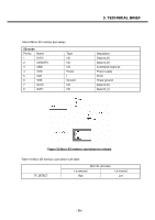
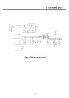
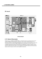
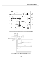
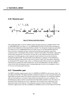
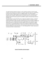
3. TECHNICAL BRIEF 3.20. Receiver part Figure 37 Receiver part block diagram The constant gain direct conversion receiver contains all active circuits for a complete receiver chain for GSM/GPRS/EDGE (see Figure 37). The GSM850/900/DCS1800/ PCS1900 LNAs with balanced inputs are fully integrated. No inter-stage filtering is needed. The orthogonal LO signals are generated by a divider-by-four for GSM850/900 band and a divider-by-two for the DCS1800/PCS1900 band. Down conversion to baseband domain is performed by low/high band quadrature direct down conversion mixers. The baseband chain contains a LNB (low noise buffer), channel filter, output buffer and DC-offset compensation. The 3rd order low pass filter is fully integrated and provides sufficient suppression of blocking signals as well as adjacent channel interferers and avoids anti-aliasing through the baseband ADC. The receive path is fully differential to suppress on-chip interferences. Several gain steps are implemented to cope with the dynamic range of the input signals. Depending on the baseband ADC dynamic range, single- or multiple gain step switching schemes are applicable. Furthermore an automatic DC-offset compensation can be used (depending on the gain setting) to reduce the DC-offset at baseband-output. A programmable gain correction can be applied to correct for front end- and receiver gain tolerances. 3.21. Transmitter part The GMSK transmitter supports power class 4 for GSM850 and GSM900 as well as power class 1 for DCS1800 and PCS1900. The digital transmitter architecture is based on a very low power fractional-N Sigma-Delta synthesizer without any external components (see Figure39). The analog I/Q modulation data from the baseband is converted to digital, filtered and transformed to polar coordinates. The phase/frequency signal is further on processed by the Sigma-Delta modulation loop. The output of its associated VCO is divided by four or two, respectively, and connected via an output buffer to the appropriate single ended output pin. This configuration ensures minimum noise level. The 8PSK transmitter supports power class E2 for GSM850 and GSM900 as well as for DCS1800 and PCS1900. - 64 -
-
 1
1 -
2
-
3
-
4
-
5
-
6
-
7
-
8
-
9
-
10
-
11
-
12
-
13
-
14
-
15
-
16
-
17
-
18
-
19
-
20
-
21
-
22
-
23
-
24
-
25
-
26
-
27
-
28
-
29
-
30
-
31
-
32
-
33
-
34
-
35
-
36
-
37
-
38
-
39
-
40
-
41
-
42
-
43
-
44
-
45
-
46
-
47
-
48
-
49
-
50
-
51
-
52
-
53
-
54
-
55
-
56
-
57
-
 58
58 -
 59
59 -
 60
60 -
 61
61 -
 62
62 -
 63
63 -
 64
64 -
 65
65 -
 66
66 -
 67
67 -
 68
68 -
69
-
70
-
71
-
72
-
73
-
74
-
75
-
76
-
77
-
78
-
79
-
80
-
81
-
82
-
83
-
84
-
85
-
86
-
87
-
88
-
89
-
90
-
91
-
92
-
93
-
94
-
95
-
96
-
97
-
98
-
99
-
100
-
101
-
102
-
103
-
104
-
105
-
106
-
107
-
108
-
109
-
110
-
111
-
112
-
113
-
114
-
115
-
116
-
117
-
118
-
119
-
120
-
121
-
122
-
123
-
124
-
125
-
126
-
127
-
128
-
129
-
130
-
131
-
132
-
133
-
134
-
135
-
136
-
137
-
138
-
139
-
140
-
141
-
142
-
143
-
144
-
145
-
146
-
147
-
148
-
149
-
150
-
151
-
152
-
153
-
154
-
155
-
156
-
157
-
158
-
159
-
160
-
161
-
162
-
163
-
164
-
165
-
166
-
167
-
168
 |
 |
