LG KE600 Service Manual - Page 64
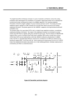
Transmitter part block diagram
 |
View all LG KE600 manuals
Add to My Manuals
Save this manual to your list of manuals |
Page 64 highlights
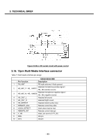
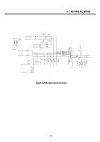
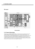
3. TECHNICAL BRIEF The digital transmitter architecture is based on a polar modulation architecture, where the analog modulation data (rectangular I/Q coordinates) is converted to digital data stream and is subsequently transformed to polar coordinates by means of a CORDIC algorithm. The resulting amplitude information is fed into a digital multiplier for power ramping and level control. The ready processed amplitude signal is applied to a DAC followed by a low pass filter which reconstructs the analog amplitude information. The phase signal from the CORDIC is applied to the Sigma-Delta fractional-N modulation loop. The divided output of its associated VCO is fed to a highly linear amplitude modulator, recombining amplitude and phase information. The output of the amplitude modulator is connected to a single ended output RF PGA for digitally setting the wanted transmit power. The PA interface of SMARTi-PM supports direct control of standard dual mode power amplifiers (PA's) which usually have a power control input VAPC and an optional bias control pin VBIAS for efficiency enhancement. In GMSK mode, the PA is in saturated high efficiency mode and is controlled via its VAPC pin directly by the baseband ramping DAC. In this way both up- / down-ramping and output power level are set. In 8PSK mode, the ramping functionality is assured by an on-chip ramping generator, whereas output power is controlled by the PGA's as described above. Figure 38 Transmitter part block diagram - 65 -
-
 1
1 -
2
-
3
-
4
-
5
-
6
-
7
-
8
-
9
-
10
-
11
-
12
-
13
-
14
-
15
-
16
-
17
-
18
-
19
-
20
-
21
-
22
-
23
-
24
-
25
-
26
-
27
-
28
-
29
-
30
-
31
-
32
-
33
-
34
-
35
-
36
-
37
-
38
-
39
-
40
-
41
-
42
-
43
-
44
-
45
-
46
-
47
-
48
-
49
-
50
-
51
-
52
-
53
-
54
-
55
-
56
-
57
-
58
-
 59
59 -
 60
60 -
 61
61 -
 62
62 -
 63
63 -
 64
64 -
 65
65 -
 66
66 -
 67
67 -
 68
68 -
 69
69 -
70
-
71
-
72
-
73
-
74
-
75
-
76
-
77
-
78
-
79
-
80
-
81
-
82
-
83
-
84
-
85
-
86
-
87
-
88
-
89
-
90
-
91
-
92
-
93
-
94
-
95
-
96
-
97
-
98
-
99
-
100
-
101
-
102
-
103
-
104
-
105
-
106
-
107
-
108
-
109
-
110
-
111
-
112
-
113
-
114
-
115
-
116
-
117
-
118
-
119
-
120
-
121
-
122
-
123
-
124
-
125
-
126
-
127
-
128
-
129
-
130
-
131
-
132
-
133
-
134
-
135
-
136
-
137
-
138
-
139
-
140
-
141
-
142
-
143
-
144
-
145
-
146
-
147
-
148
-
149
-
150
-
151
-
152
-
153
-
154
-
155
-
156
-
157
-
158
-
159
-
160
-
161
-
162
-
163
-
164
-
165
-
166
-
167
-
168
 |
 |
