LG KE990 Service Manual - Page 24
GSM PAM U101:TQM7M5003
 |
View all LG KE990 manuals
Add to My Manuals
Save this manual to your list of manuals |
Page 24 highlights
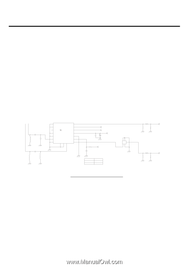
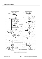
3. TECHNICAL BRIEF 3.4.4 GSM PAM (U101:TQM7M5003) The TQM7M5003 is an extremely small (7 x 7 mm), GSM/EDGE PAM for handset applications. This module has been optimized for excellent EDGE efficiency and Pout in a Polar Loop environment at EDGE class E2+ operation while maintaining high GSM/GPRS efficiency. The small size and high performance is achieved with high-reliability 3 rd generation InGaP HBT technology. With 50Ω and output, no external matching or bias components are required. The module incorporates two highly-integrated InGaP power amplifier die with a CMOS controller. Each amplifier has three gain stages with on-die inter-stage matching implemented with a high Q passives technology for optimal performance. The CMOS controller implements a fully integrated power control within the module for GSM operations, and serves as the AM/AM path in EDGE operations. This eliminates the need for any external couplers, power detectors, current sensing etc., to assure the output power level. The module has Tx enable and band select inputs. Module construction is a low-profile overmolded landgrid array on laminate. C136 6.8p L112 15nH C138 NA C146 2.7p C142 5.6nH L113 5.6nH 17 GND8 16 GND7 15 DCS_PCS_OUT 14 GND6 DCS_PCS_IN 1 13 GND5 BS 2 12 VCC 11 GND4 U101 TQM7M5003 3 TX_EN 4 VBATT 10 GND3 GND1 5 9 GSM_OUT VRAMP 6 8 GND2 GSM_IN 7 GSM_PA_BAND GSM_PA_EN C137 C135 1u 33u +VPWR R117 2.2K C143 68p GSM_PA_RAMP 32 G2 G1 IN O1 G3 1 45 EFCH836MTDB1 FL101 GSM_PA_BAND MODE LOW HIGH GSM850/900 DCS/PCS [Figure 3.4.4] GSM PAM Schematic R112 100 R111 68 10 dB R113 100 DCS_PCS_TX R114 68 R118 100 10dB R119 100 GSM_TX Copyright © 2008 LG Electronics. Inc. All right reserved. Only for training and service purposes - 25 - LGE Internal Use Only
-
 1
1 -
2
-
3
-
4
-
5
-
6
-
7
-
8
-
9
-
10
-
11
-
12
-
13
-
14
-
15
-
16
-
17
-
18
-
 19
19 -
 20
20 -
 21
21 -
 22
22 -
 23
23 -
 24
24 -
 25
25 -
 26
26 -
 27
27 -
 28
28 -
 29
29 -
30
-
31
-
32
-
33
-
34
-
35
-
36
-
37
-
38
-
39
-
40
-
41
-
42
-
43
-
44
-
45
-
46
-
47
-
48
-
49
-
50
-
51
-
52
-
53
-
54
-
55
-
56
-
57
-
58
-
59
-
60
-
61
-
62
-
63
-
64
-
65
-
66
-
67
-
68
-
69
-
70
-
71
-
72
-
73
-
74
-
75
-
76
-
77
-
78
-
79
-
80
-
81
-
82
-
83
-
84
-
85
-
86
-
87
-
88
-
89
-
90
-
91
-
92
-
93
-
94
-
95
-
96
-
97
-
98
-
99
-
100
-
101
-
102
-
103
-
104
-
105
-
106
-
107
-
108
-
109
-
110
-
111
-
112
-
113
-
114
-
115
-
116
-
117
-
118
-
119
-
120
-
121
-
122
-
123
-
124
-
125
-
126
-
127
-
128
-
129
-
130
-
131
-
132
-
133
-
134
-
135
-
136
-
137
-
138
-
139
-
140
-
141
-
142
-
143
-
144
-
145
-
146
-
147
-
148
-
149
-
150
-
151
-
152
-
153
-
154
-
155
-
156
-
157
-
158
-
159
-
160
-
161
-
162
-
163
-
164
-
165
-
166
-
167
-
168
-
169
-
170
-
171
-
172
-
173
-
174
-
175
-
176
-
177
-
178
-
179
-
180
-
181
-
182
-
183
-
184
-
185
-
186
-
187
-
188
-
189
-
190
-
191
-
192
-
193
-
194
-
195
-
196
-
197
-
198
-
199
-
200
-
201
-
202
-
203
-
204
 |
 |