LG KG270 Service Manual - Page 31
PAMPower Amplifier Module interface
 |
View all LG KG270 manuals
Add to My Manuals
Save this manual to your list of manuals |
Page 31 highlights
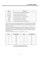
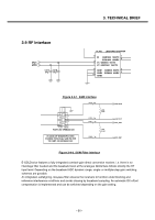
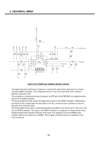
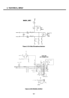
3. TECHNICAL BRIEF TX_RAMP R402 1K C401 39p (50V,J,NP0) (16V,K,X7R) (10V,Z,Y5V) (50V,J,NP0) (50V,J,NP0) VBAT VBAT C403 12p C404 C402 0.01u 10u (2012) C405 33p C406 18p C407 27p C408 0.01u VAPC 20 VBATT 17 VCC1B 6 VCC1A 2 R406 0 C411 C412 NA NA R410 0 C415 NA C416 NA 16 GND9 GND8 14 13 GND7 12 GND6 GND5 10 9 GND4 8 GND3 GND2 7 5 GND1 15 DCS_PCS_OUT DCS_PCS_IN 3 11 EGSM_OUT 19 RSVD_GND U400 SKY77318 4 EGSM_IN ENABLE 18 21 P_GND BS 1 (50V,J,NP0) (16V,K,X7R) C413 27p C414 27p R404 0 R405 0 L402 NA C409 NA DCS_PCS_OUT TXON_PA BS R407 0 R408 NA R409 NA GSM_OUT Figure 3-9-3. PAM(Power Amplifier Module) interface The digital transmitter architecture is based on a fractional-N sigma-delta synthesizer for constant envelope GMSK modulation. This configuration allows a very low power design with a reduced external component count. The modulation is transferred between baseband- and RF-part of the PMB7880 via a digital interface signal into the digital modulator. The following Gaussian filter shapes the digital data stream for the GMSK modulation. Additionally a pre-distortion filter compensates the attenuation of the PLL transfer function resulting in a very low distortion at the transmit output. The filtered digital data stream is scaled appropriately and added to the channel word. This sum is fed into the MASH modulator. The output of the MASH modulator is a sequence of integer divider values representing the high resolution fractional input signal. This sequence controls the MMD (multi modulus divider) at a sample rate of 26MHz. Thus a tightly controlled frequency modulation of the VCO is achieved. - 32 -
-
 1
1 -
2
-
3
-
4
-
5
-
6
-
7
-
8
-
9
-
10
-
11
-
12
-
13
-
14
-
15
-
16
-
17
-
18
-
19
-
20
-
21
-
22
-
23
-
24
-
25
-
 26
26 -
 27
27 -
 28
28 -
 29
29 -
 30
30 -
 31
31 -
 32
32 -
 33
33 -
 34
34 -
 35
35 -
 36
36 -
37
-
38
-
39
-
40
-
41
-
42
-
43
-
44
-
45
-
46
-
47
-
48
-
49
-
50
-
51
-
52
-
53
-
54
-
55
-
56
-
57
-
58
-
59
-
60
-
61
-
62
-
63
-
64
-
65
-
66
-
67
-
68
-
69
-
70
-
71
-
72
-
73
-
74
-
75
-
76
-
77
-
78
-
79
-
80
-
81
-
82
-
83
-
84
-
85
-
86
-
87
-
88
-
89
-
90
-
91
-
92
-
93
-
94
-
95
-
96
-
97
-
98
-
99
-
100
-
101
-
102
-
103
-
104
-
105
-
106
-
107
-
108
-
109
-
110
-
111
-
112
-
113
-
114
-
115
-
116
-
117
-
118
-
119
-
120
-
121
-
122
-
123
-
124
-
125
 |
 |
