Pioneer SX-255R Service Manual - Page 21
Pioneer SX-255R Manual
 |
View all Pioneer SX-255R manuals
Add to My Manuals
Save this manual to your list of manuals |
Page 21 highlights
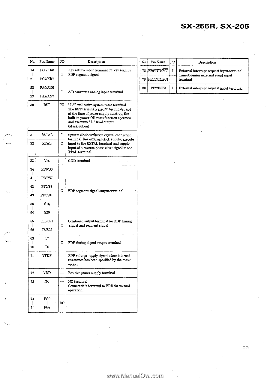
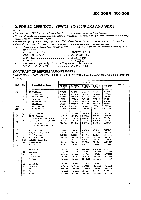
SX-255R SX-205 No. Pin Name I/O Description 14 PC0/KR0 I I 21 PC7/KR7 Key return input terminal for key scan by I FDP segment signal 22 PA0/AN0 I I 29 PA7/AN7 I A/D converter analog input terminal 30 RST I/O " L " level active system reset terminal. The RST terminals are I/O terminals, and at the time of power supply start-up, the built-in power ON reset function operates and executes " L " level output. (Mask option) 31 EXTAL 32 XTAL I System clock oscillstion crystal connection terminal. For external clock supply, execute O input to the EXTAL terminal and supply input of a reverse-phase clock signal to the XTAL terminal. 33 Vss - GND terminal 34 PD0/SO I I 41 PD7/S7 42 PF0/S8 I I 49 PF7/S15 O FDP segment signal output terminal 50 S16 I I 54 S20 55 T15/S21 Combined output terminal for FDP timing I I O signal and segment signal 62 T8/S28 63 T7 ,I I O FDP timing signal output terminal 70 TO 71 VFDP - FDP voltage supply signal when internal resistance has been specified by the mask option. 72 VDD - Positive power supply terminal 73 NC - NC terminal Connect this terminal to VDD for normal operation. 74 PG0 I I I/O 77 PG3 No. Pin Name 1/O Description 78 PEO/IN'l'0/ECO I 79 PEVINTIJEC1 External interrupt request input terminal Timer/counter external event input terminal 80 PE2/INT2 I External interrupt request input terminal 29
-
 1
1 -
2
-
3
-
4
-
5
-
6
-
7
-
8
-
9
-
10
-
11
-
12
-
13
-
14
-
15
-
 16
16 -
 17
17 -
 18
18 -
 19
19 -
 20
20 -
 21
21 -
 22
22 -
 23
23 -
 24
24 -
 25
25 -
 26
26 -
27
-
28
-
29
 |
 |