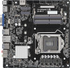
ASRock H510TM-ITX User Manual - Page 43
DRAM Timing Configuration
 |
View all ASRock H510TM-ITX manuals
Add to My Manuals
Save this manual to your list of manuals |
Page 43 highlights
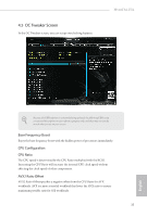
DRAM Configuration Memory Information Allows users to browse the serial presence detect (SPD) and Intel extreme memory profile (XMP) for DDR4 modules. DRAM Timing Configuration Load XMP Setting Load XMP settings to overclock the memory and perform beyond standard specifications. DRAM Reference Clock Select Auto for optimized settings. DRAM Frequency If [Auto] is selected, the motherboard will detect the memory module(s) inserted and assign the appropriate frequency automatically. DRAM Gear Mode Gear2 mode doubled the ratio in memory controller, and it is good for high frequency. Primary Timing CAS# Latency (tCL) The time between sending a column address to the memory and the beginning of the data in response. RAS# to CAS# Delay and Row Precharge (tRCDtRP) RAS# to CAS# Delay : The number of clock cycles required between the opening of a row of memory and accessing columns within it. Row Precharge: The number of clock cycles required between the issuing of the precharge command and opening the next row. RAS# Active Time (tRAS) The number of clock cycles required between a bank active command and issuing the precharge command. Command Rate (CR) The delay between when a memory chip is selected and when the first active command can be issued. 38 English
-
 1
1 -
2
-
3
-
4
-
5
-
6
-
7
-
8
-
9
-
10
-
11
-
12
-
13
-
14
-
15
-
16
-
17
-
18
-
19
-
20
-
21
-
22
-
23
-
24
-
25
-
26
-
27
-
28
-
29
-
30
-
31
-
32
-
33
-
34
-
35
-
36
-
37
-
 38
38 -
 39
39 -
 40
40 -
 41
41 -
 42
42 -
 43
43 -
 44
44 -
 45
45 -
 46
46 -
 47
47 -
 48
48 -
49
-
50
-
51
-
52
-
53
-
54
-
55
-
56
-
57
-
58
-
59
-
60
-
61
-
62
-
63
-
64
-
65
-
66
-
67
-
68
-
69
 |
 |
