ASRock X99 Extreme4 User Manual - Page 68
RAS to RAS Delay tRRD_L
 |
View all ASRock X99 Extreme4 manuals
Add to My Manuals
Save this manual to your list of manuals |
Page 68 highlights
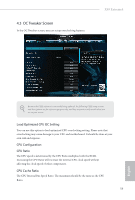
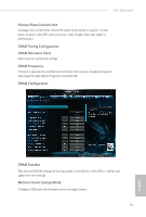
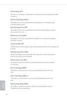
CAS# Latency (tCL) he time between sending a column address to the memory and the beginning of the data in response. RAS# to CAS# Delay (tRCD) he number of clock cycles required between the opening of a row of memory and accessing columns within it. Row Precharge Time (tRP) he number of clock cycles required between the issuing of the precharge command and opening the next row. RAS# Active Time (tRAS) he number of clock cycles required between a bank active command and issuing the precharge command. Command Rate (CR) he delay between when a memory chip is selected and when the irst active command can be issued. Write Recovery Time (tWR) he amount of delay that must elapse ater the completion of a valid write operation, before an active bank can be precharged. Refresh Cycle Time (tRFC) he number of clocks from a Refresh command until the irst Activate command to the same rank. RAS to RAS Delay (tRRD) he number of clocks between two rows activated in diferent banks of the same rank. RAS to RAS Delay (tRRD_L) he number of clocks between two rows activated in diferent banks of the same rank. Write to Read Delay (tWTR) he number of clocks between the last valid write operation and the next read command to the same internal bank. 62 English
-
 1
1 -
2
-
3
-
4
-
5
-
6
-
7
-
8
-
9
-
10
-
11
-
12
-
13
-
14
-
15
-
16
-
17
-
18
-
19
-
20
-
21
-
22
-
23
-
24
-
25
-
26
-
27
-
28
-
29
-
30
-
31
-
32
-
33
-
34
-
35
-
36
-
37
-
38
-
39
-
40
-
41
-
42
-
43
-
44
-
45
-
46
-
47
-
48
-
49
-
50
-
51
-
52
-
53
-
54
-
55
-
56
-
57
-
58
-
59
-
60
-
61
-
62
-
 63
63 -
 64
64 -
 65
65 -
 66
66 -
 67
67 -
 68
68 -
 69
69 -
 70
70 -
 71
71 -
 72
72 -
 73
73 -
74
-
75
-
76
-
77
-
78
-
79
-
80
-
81
-
82
-
83
-
84
-
85
-
86
-
87
-
88
-
89
-
90
-
91
-
92
-
93
-
94
 |
 |