ASRock Z690 PG Velocita User Manual - Page 91
ODT NOM Rd B1
 |
View all ASRock Z690 PG Velocita manuals
Add to My Manuals
Save this manual to your list of manuals |
Page 91 highlights
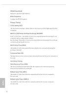
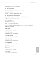
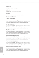
Z690 PG Velocita ODT WR (A2) Configure the memory on die termination resistors' WR for channel A2. ODT WR (B1) Configure the memory on die termination resistors' WR for channel B1. ODT WR (B2) Configure the memory on die termination resistors' WR for channel B2. ODT NOM Rd (A1) Configure the memory on die termination resistors' NOM Rd for channel A1. ODT NOM Rd (A2) Configure the memory on die termination resistors' NOM Rd for channel A2. ODT NOM Rd (B1) Configure the memory on die termination resistors' NOM Rd for channel B1. ODT NOM Rd (B2) Configure the memory on die termination resistors' NOM Rd for channel B2. ODT NOM Wr (A1) Configure the memory on die termination resistors' NOM Wr for channel A1. ODT NOM Wr (A2) Configure the memory on die termination resistors' NOM Wr for channel A2. ODT NOM Wr (B1) Configure the memory on die termination resistors' NOM Wr for channel B1. ODT NOM Wr (B2) Configure the memory on die termination resistors' NOM Wr for channel B2. ODT PARK (A1) Configure the memory on die termination resistors' PARK for channel A1. ODT PARK (A2) Configure the memory on die termination resistors' PARK for channel A2. 83 English
-
 1
1 -
2
-
3
-
4
-
5
-
6
-
7
-
8
-
9
-
10
-
11
-
12
-
13
-
14
-
15
-
16
-
17
-
18
-
19
-
20
-
21
-
22
-
23
-
24
-
25
-
26
-
27
-
28
-
29
-
30
-
31
-
32
-
33
-
34
-
35
-
36
-
37
-
38
-
39
-
40
-
41
-
42
-
43
-
44
-
45
-
46
-
47
-
48
-
49
-
50
-
51
-
52
-
53
-
54
-
55
-
56
-
57
-
58
-
59
-
60
-
61
-
62
-
63
-
64
-
65
-
66
-
67
-
68
-
69
-
70
-
71
-
72
-
73
-
74
-
75
-
76
-
77
-
78
-
79
-
80
-
81
-
82
-
83
-
84
-
85
-
 86
86 -
 87
87 -
 88
88 -
 89
89 -
 90
90 -
 91
91 -
 92
92 -
 93
93 -
 94
94 -
 95
95 -
 96
96 -
97
-
98
-
99
-
100
-
101
-
102
-
103
-
104
-
105
-
106
-
107
-
108
-
109
-
110
-
111
-
112
-
113
-
114
-
115
-
116
-
117
-
118
-
119
-
120
-
121
-
122
-
123
-
124
-
125
-
126
-
127
-
128
 |
 |