Asus A7VL133-VM Motherboard DIY Troubleshooting Guide - Page 59
data. Configuration options: [4MB] [8MB] [16MB] [32MB] [64MB]
 |
View all Asus A7VL133-VM manuals
Add to My Manuals
Save this manual to your list of manuals |
Page 59 highlights
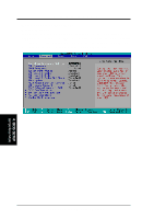
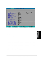
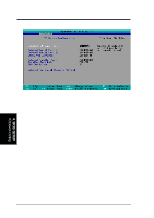
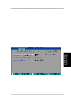
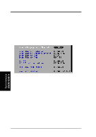
4. BIOS SETUP Byte Merge [Disabled] To optimize the data transfer on PCI, this merges a sequence of individual memory writes (bytes or words) into a single 32-bit block of data. However, byte merging may only be done when the bytes within a data phase are in a prefetchable address range. Configuration options: [Disabled] [Enabled] DRAM Read Latch Delay [Auto] Configuration options: [-0.01 ns] [0.75 ns] [1.72 ns] [2.69 ns] [-0.01 ns] [2.11 ns] [3.08 ns] [4.05 ns]...[Auto] Memory Early/Delay Write [Auto] Configuration options: [0.0 ns] [0.5 ns] [1.0 ns] [1.5 ns] [-0.5 ns] [-1.0 ns] [-1.5 ns] [Auto] DIMM Interleave Setting [Auto] Configuration options: [Auto] [Disabled] Graphics Aperture Size [64MB] This feature allows you to select the size of mapped memory for AGP graphic data. Configuration options: [4MB] [8MB] [16MB] [32MB] [64MB] [128MB] [256MB] VGA Shared Memory Size [16MB] Configuration options: [8MB] [16MB] [32MB] Video Memory Cache Mode [UC] USWC (uncacheable, speculative write combining) is a new cache technology for the video memory of the processor. It can greatly improve the display speed by caching the display data. You must set this to UC (uncacheable) if your display card cannot support this feature; otherwise your system may not boot. Configuration options: [UC] [USWC] 4. BIOS SETUP ASUS A7VL133-VM User's Manual 59
-
 1
1 -
2
-
3
-
4
-
5
-
6
-
7
-
8
-
9
-
10
-
11
-
12
-
13
-
14
-
15
-
16
-
17
-
18
-
19
-
20
-
21
-
22
-
23
-
24
-
25
-
26
-
27
-
28
-
29
-
30
-
31
-
32
-
33
-
34
-
35
-
36
-
37
-
38
-
39
-
40
-
41
-
42
-
43
-
44
-
45
-
46
-
47
-
48
-
49
-
50
-
51
-
52
-
53
-
 54
54 -
 55
55 -
 56
56 -
 57
57 -
 58
58 -
 59
59 -
 60
60 -
 61
61 -
 62
62 -
 63
63 -
 64
64 -
65
-
66
-
67
-
68
-
69
-
70
-
71
-
72
-
73
-
74
-
75
-
76
-
77
-
78
-
79
-
80
-
81
-
82
-
83
-
84
-
85
-
86
-
87
-
88
-
89
-
90
-
91
-
92
-
93
-
94
-
95
-
96
 |
 |