Asus HX97 User Manual - Page 43
Onboard FDC Swap A & B No Swap
 |
View all Asus HX97 manuals
Add to My Manuals
Save this manual to your list of manuals |
Page 43 highlights
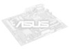
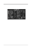
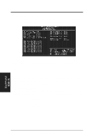
IV. BIOS SOFTWARE Video BIOS Cacheable (Enabled) Allows the Video BIOS to be cached to allow faster execution. Leave on default setting of Enabled for better performance, otherwise Disabled. Memory Hole at 15M - 16M Enabling this features reserves 15MB to 16MB memory address space to ISA expansion cards that specifically require this setting. This makes the memory from 15MB and up unavailable to the system. Expansion cards can only access memory up to 16MB. The default is Disabled. [DRAM and ECC] If all your DRAM modules have parity chips (e.g. 8 chips + 4 parity chips), they are considered 36bits. This motherboard sums the memory per bank and therefore two modules will give 72bits and the following will be displayed: If your DRAM modules do not have parity chips (e.g. 8 chips), they are considered 32bits and the following will be displayed instead: The default of Disabled for Memory parity SERR# (NMI) will not show memory errors on your monitor. When using parity DRAM modules, you can select from the default of Parity or ECC (Error Checking and Correcting) to correct 1 bit memory errors that may occur in the memory. (See pages 12-13 for more information on DRAM memory modules.) ...Onboard FDC Controller (Enabled) When enabled, this field allows you to connect your floppy disk drives to the onboard floppy drive connector instead of a separate controller card. If you want to use a different controller card to connect the floppy drives, set this field to Disabled. Onboard FDC Swap A & B (No Swap) This field reverses the drive letter assignments of your floppy disk drives. Two options are available: No Swap and Swap AB. If you want to switch drive letter assignments, set this field to Swap AB, and the swap will be controlled in hardware. This works separately from the BIOS Features floppy disk swap feature. It is functionally the same as physically interchanging the connectors of the floppy disk drives. IV. BIOS (Chipset Features) ASUS HX97 User's Manual 43
-
 1
1 -
2
-
3
-
4
-
5
-
6
-
7
-
8
-
9
-
10
-
11
-
12
-
13
-
14
-
15
-
16
-
17
-
18
-
19
-
20
-
21
-
22
-
23
-
24
-
25
-
26
-
27
-
28
-
29
-
30
-
31
-
32
-
33
-
34
-
35
-
36
-
37
-
 38
38 -
 39
39 -
 40
40 -
 41
41 -
 42
42 -
 43
43 -
 44
44 -
 45
45 -
 46
46 -
 47
47 -
 48
48 -
49
-
50
-
51
-
52
-
53
-
54
-
55
-
56
-
57
-
58
-
59
-
60
-
61
-
62
-
63
-
64
 |
 |