Asus SP98AGP-X SP98AGP-X User Manual - Page 45
MB-16MB, 14MB-16MB, 15MB-16MB, Enabled, Disabled, Swap AB, No Swap, 3F8H/IRQ4, 2F8H/IRQ3, 3E8H/
 |
View all Asus SP98AGP-X manuals
Add to My Manuals
Save this manual to your list of manuals |
Page 45 highlights
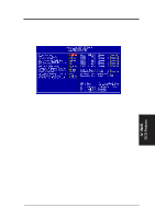
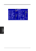
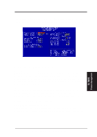
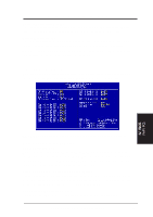
BIOS Features IV. BIOS SOFTWARE Graphics Aperture Size (64MB) (Leave on default setting of 64MB) Memory-mapped, graphics data structures can reside in a Graphics Aperture. Memory Hole at Address (None) This features reserves either 12MB-16MB, 14MB-16MB, or 15MB-16MB memory address space to ISA expansion cards that specifically require this setting. Memory from either 12MB and up, 14MB and up, or 15MB and up will be unavailable to the system because expansion cards can only access memory up to 16MB. Refresh Queue Depth (12) This function sets the DRAM refresh rate. A slow refresh cycle time increases the bandwidth available for data transfers. NOTE: Some DRAMs are known to lose data without frequent refreshing so the default is set at 0. Delayed Transaction (Enabled) The default setting of Enabled frees the PCI Bus during CPU accessing of 8-bit ISA cards, which normally consume about 50-60 PCI clocks without PCI delayed transaction. For PCI bus masters that cannot use the PCI Bus and some ISA cards that are not PCI 2.1 compliant, set this to Disabled. DRAM are 64 (Not 72) bits wide This motherboard does not have parity support, thus DRAM modules are always 64 bits wide. Data Integrity Mode (None) The setting None has byte-wise write capability but no provision for protecting data integrity in the DRAM array. You can enable the ECC function if ECC-supported DIMM is used. (See section III for more information on memory modules.) ...Onboard FDC Controller (Enabled) When enabled, this field allows you to connect your floppy disk drives to the onboard floppy drive connector instead of a separate controller card. If you want to use a different controller card to connect the floppy drives, set this field to Disabled. Onboard FDC Swap A & B (No Swap) This field allows you to reverse the hardware drive letter assignments of your floppy disk drives through the onboard chipset. If you want to switch drive letter assignments, set this field to Swap AB. Default setting is No Swap. Onboard Serial Port 1 (3F8H/IRQ4) and Onboard Serial Port 2 (2F8H/IRQ3) Settings are 3F8H/IRQ4, 2F8H/IRQ3, 3E8H/IRQ4, 2E8H/IRQ10, and Disabled for the onboard serial connectors. Default setting for Serial Port 1 is 3F8H/IRQ4, while for Serial Port 2 is 2F8H/IRQ3. IV. BIOS Chipset Features ASUS SP98AGP-X User's Manual 45
-
 1
1 -
2
-
3
-
4
-
5
-
6
-
7
-
8
-
9
-
10
-
11
-
12
-
13
-
14
-
15
-
16
-
17
-
18
-
19
-
20
-
21
-
22
-
23
-
24
-
25
-
26
-
27
-
28
-
29
-
30
-
31
-
32
-
33
-
34
-
35
-
36
-
37
-
38
-
39
-
 40
40 -
 41
41 -
 42
42 -
 43
43 -
 44
44 -
 45
45 -
 46
46 -
 47
47 -
 48
48 -
 49
49 -
 50
50 -
51
-
52
-
53
-
54
-
55
-
56
-
57
-
58
-
59
-
60
-
61
-
62
-
63
-
64
 |
 |
