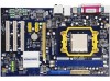
Foxconn 560A multilateral manual. - Page 30
Trcd RAS to CAS R/W Delay
 |
View all Foxconn 560A manuals
Add to My Manuals
Save this manual to your list of manuals |
Page 30 highlights
Chapter 2 BIOS Description (Trc)Row Cycle Time Allows you to set the minimum time interval between successive active commands to the same bank. (Trcd) RAS to CAS R/W Delay Allows you to set the number of clock cycles taken between the issuing of the active command and the read/write command. (Trrd) RAS to RAS Delay Allows you to set the minimum time interval between successive active commands to the different banks. (Trp) ROW Precharge Time Allows you to set the number of clock cycles taken between the issuing of the precharge command and the active command. (Tras) Min.RAS Active Time Allows you to set the number of clock cycles taken between a bank active command and issuing the precharge command. 2.8 CPU/PCIE Spread Spectrum W hen enabled, it can significantly reduce the EMI (Electromagnetic Interference). 2.9 PCIE Clock This option is used to set PCI Express Clock. 2.10 AMD K8 Cool & Quiet Control This option helps the system to lower the frequency when CPU idles.W hen the frequency decreases, the temperature will drop automatically as well. 2.11 Vcore Voltage Select This option is used to select the vcore voltage based on the default voltage. The value can be set from "-0.05V" to "+0.325V", the step value is "0.025V". 2.12 DRAM Voltage Select This option is used to select the DRAM voltage based on the default voltage. The value can be set from "-0.15V" to "+0.6V", the step value is "0.05V". 2.13 Chipset Voltage Select This option is used to select the chipset voltage based on the default voltage. The value can be set from "-0.12V" to "+0.2V", the step value is "0.04V". 2.14 LDT Voltage Select This option is used to select the LDT voltage based on the default voltage. The value can be set from "-0.09V" to "+0.36V", the step value is "0.03V". 25
-
 1
1 -
2
-
3
-
4
-
5
-
6
-
7
-
8
-
9
-
10
-
11
-
12
-
13
-
14
-
15
-
16
-
17
-
18
-
19
-
20
-
21
-
22
-
23
-
24
-
 25
25 -
 26
26 -
 27
27 -
 28
28 -
 29
29 -
 30
30 -
 31
31 -
 32
32 -
 33
33 -
 34
34 -
 35
35 -
36
-
37
-
38
-
39
-
40
-
41
-
42
-
43
-
44
-
45
-
46
 |
 |
