Foxconn 720AL English Manual. - Page 35
► [Trcd] RAS to CAS R/W Delay
 |
View all Foxconn 720AL manuals
Add to My Manuals
Save this manual to your list of manuals |
Page 35 highlights
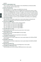
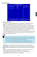
3 disabled. ► Bottom of UMA DRAM [31:24] This is a memory allocation method addition to the Unified Memory Architecture (UMA) concept. Normally, select the default value. ► Memory Timing Setting Select [Enabled], you can configure the DRAM timing manually. Select [Disabled], then system will use the DRAM timing provided by the memory vendor. The provision of DRAM timing is done by a SPD device. The Serial Presence Detect (SPD) device is a small EEPROM chip, mounted on a DDR2 memory module. It contains important information about the module's speed, size, addressing mode and various other parameters, so that the motherboard memory controller (chipset) can better access the memory device. The following 8 settings are valid only when the DRAM Timing Setting is set to [Enabled]. ► TwTr Command Delay This item allows you to select a delay time (in clock cycles) between sending the last data from a write operation to the memory and issuing a read command. ► Trfc0/1/2/3 for DIMM0/1/2/3 Refresh to Refresh or Refresh to Active command interval. Trfc3: auto-refresh row cycle time for logical DIMM 3 Trfc2: auto-refresh row cycle time for logical DIMM 2 Trfc1: auto-refresh row cycle time for logical DIMM 1 Trfc0: auto-refresh row cycle time for logical DIMM 0 ► [Twr] Write Recovery Time This item allows you to select the write recovery time (in clock cycles). ► [Trtp] Precharge Time Internal READ Command to PRECHARGE Command delay. ► [Trc] Row Cycle Time This item allows you to set the row cycle time (in clock cycles). ► [Trcd] RAS to CAS R/W Delay This item allows you to select a delay time (in clock cycles) between the CAS# and RAS# strobe signals. ► [Trrd] Ras to RAS Delay This item allows you to select a delay time (in clock cycles) between the RAS# and RAS# strobe signals. ► [Trp] Row Precharge Time This item allows you to select the row precharge time (in clock cycles). ► [Tras] Minimum RAS Active Time This item allows you to set the minimum RAS# active time (in clock cycles). 28
-
 1
1 -
2
-
3
-
4
-
5
-
6
-
7
-
8
-
9
-
10
-
11
-
12
-
13
-
14
-
15
-
16
-
17
-
18
-
19
-
20
-
21
-
22
-
23
-
24
-
25
-
26
-
27
-
28
-
29
-
 30
30 -
 31
31 -
 32
32 -
 33
33 -
 34
34 -
 35
35 -
 36
36 -
 37
37 -
 38
38 -
 39
39 -
 40
40 -
41
-
42
-
43
-
44
-
45
-
46
-
47
-
48
-
49
-
50
-
51
-
52
-
53
-
54
-
55
-
56
-
57
-
58
-
59
-
60
-
61
-
62
-
63
-
64
-
65
-
66
-
67
-
68
-
69
-
70
-
71
-
72
-
73
-
74
-
75
-
76
-
77
-
78
-
79
-
80
-
81
-
82
-
83
-
84
-
85
-
86
-
87
-
88
-
89
-
90
-
91
-
92
-
93
-
94
-
95
-
96
-
97
-
98
-
99
-
100
-
101
-
102
-
103
-
104
-
105
-
106
-
107
-
108
-
109
-
110
 |
 |