HP DL740 HP F8 Architecture Technology Brief - Page 4
Overview of F8 Chipset, 2GB/s, 400 MT/s, bit, 100-MHz, PCI-X Hot Plug, SDRAM, Aggregate - pci memory controller
 |
UPC - 808736765770
View all HP DL740 manuals
Add to My Manuals
Save this manual to your list of manuals |
Page 4 highlights
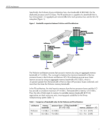
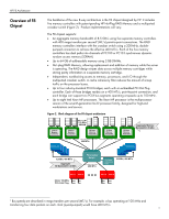
HP F8 Architecture Overview of F8 Chipset The backbone of the new 8-way architecture is the F8 chipset designed by HP. It includes five memory controllers with patent-pending HP Hot-Plug RAID Memory and a multiported crossbar switch (Figure 2). Product implementations will vary. The F8 chipset supports: • An aggregate memory bandwidth of 8.5 GB/s using five separate memory controllers with 400 mega transfers per second3 (MT/s) point-to-point connections. The RAID memory controllers interface with the crossbar switch using a 200-MHz, doublepumped connection to achieve the effective 400 MT/s. Each of the five memory controllers has dual paths into channels of PC100 or PC133 synchronous dynamic random access memory (SDRAM). • Up to 64 GB of addressable memory using 2-GB DIMMs. • Hot -plug RAID Memory, allowing replacement and addition of memory while the server is operating. The RAID design stripes data across multiple memory cartridges while storing parity information in a separate memory cartridge. • Independent, nonblocking access to memory, processors, and I/O through the multiported crossbar switch. A cache coherency filter reduces the amount of snoop traffic on the processor buses. • Up to four industry-standard PCI-X bridges, each with an embedded PCI Hot Plug controller. Each of these bridges resides on a 400 MT/s, point-to-point connection, and each bridge can support two PCI-X bus segments operating at speeds up to 100 MHz. • Up to eight Intel Xeon MP processors. The Xeon MP processor is the multiprocessor version of the seventh-generation IA-32 processor family, designed for high-end workstations and servers. Figure 2. Block diagram of the F8 chipset architecture FF88DDuuaal l MMeemmooryry CCoonnttrroolllleerr Processors 133-MHz SDRAM FF88DDuuaal l MMeemmoorryy CCoonnttrroolllleerr FF88DDuuaal l MMeemmooryry CCoonnttrroolllleerr 400 MT/s FF88DDuuaal l MMeemmooryry CCoonnttrroolllleerr FF88DDuuaal l MMeemmooryry CCoonnttrroolllleerr Aggregate Memory Bandwidth 8.5 GB/s Processors 3.2GB/s, 400 MT/s Aggregate I/O Bandwidth 3.2 GB/s FF88CCrroossssbbaar r SSwwiittcchh 400 MT/s F8 Cache Coherency Filter 3.2GB/s, 400 MT/s PPCCII-X PPCCI-IX-X 64-bit, 100-MHz PCI-X Hot Plug PPCCI-IX-X PPCCI-XI-X 3 Bus speeds are described in mega transfers per second (MT/s). For example, a bus operating at 100 MHz and transferring four data packets on each clock (quad-pumped) would have 400 MT/s. 4
-
 1
1 -
 2
2 -
 3
3 -
 4
4 -
 5
5 -
 6
6 -
 7
7 -
 8
8 -
 9
9 -
 10
10 -
11
-
12
-
13
-
14
 |
 |
