Hitachi DK23BA-20 Owners Manual - Page 101
Symbol Min Max Min Max Min Max Min Max Min Max Min
 |
View all Hitachi DK23BA-20 manuals
Add to My Manuals
Save this manual to your list of manuals |
Page 101 highlights
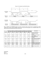
DSTROBE at device DD(15:0) at device Figure 6-9 Sustained Ultra DMA Read Data tCYC t2CYC tCYC tDVH tDVHIC tDVS tDVSIC tDVH tDVHIC tDVS tDVSIC tDVH tDVHIC t2CYC DSTROBE at host DD(15:0) at host tDH tDHIC tDS tDSIC tDH tDHIC tDS tDSIC tDH tDHIC Note: DD(15:0) and DSTROBE signals are shown at both the host and the device to emphasize that cable settling time as well as cable propagation delay shall not allow the data signals to be considered stable at the host until some time after they are driven by the device. SYMBOL tCYC t2CYC tDS tDH tDVS tDVH tDSIC tDHIC tDVSIC tDVHIC Mode 0(ns) Mode 1(ns) Mode 2(ns) Mode3(ns) Mode4(ns) MIN MAX MIN MAX MIN MAX MIN MAX MIN MAX 112 73 54 39 25 230 153 115 86 57 15 10 7 7 5 5 5 5 5 5 70 48 31 20 6.7 6.2 6.2 6.2 6.2 6.2 14.7 9.7 6.8 6.8 4.8 4.8 4.8 4.8 4.8 4.8 72.9 50.9 33.9 22.6 9.5 9.0 9.0 9.0 9.0 9.0 Mode5(ns) MIN MAX 16.8 38 4 4.6 4.8 4.8 2.3 2.8 6.0 6.0 Description Cycle time allowing for asymmetry and clock variation Two cycle time allowing for clock variation Data setup time at recipient Data hold time at recipient Data valid setup time at sender Data valid hold time at sender Recipient IC data setup time Recipient IC data hold time Sender IC data valid setup time Sender IC data valid hold time K6610007 Rev.5 02.14.'03 - 101 -
-
 1
1 -
2
-
3
-
4
-
5
-
6
-
7
-
8
-
9
-
10
-
11
-
12
-
13
-
14
-
15
-
16
-
17
-
18
-
19
-
20
-
21
-
22
-
23
-
24
-
25
-
26
-
27
-
28
-
29
-
30
-
31
-
32
-
33
-
34
-
35
-
36
-
37
-
38
-
39
-
40
-
41
-
42
-
43
-
44
-
45
-
46
-
47
-
48
-
49
-
50
-
51
-
52
-
53
-
54
-
55
-
56
-
57
-
58
-
59
-
60
-
61
-
62
-
63
-
64
-
65
-
66
-
67
-
68
-
69
-
70
-
71
-
72
-
73
-
74
-
75
-
76
-
77
-
78
-
79
-
80
-
81
-
82
-
83
-
84
-
85
-
86
-
87
-
88
-
89
-
90
-
91
-
92
-
93
-
94
-
95
-
 96
96 -
 97
97 -
 98
98 -
 99
99 -
 100
100 -
 101
101 -
 102
102 -
 103
103 -
 104
104 -
 105
105 -
 106
106 -
107
-
108
-
109
-
110
-
111
-
112
-
113
-
114
 |
 |
