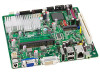
Intel BLKD945GSEJT Product Guide - Page 41
Add-in Card Connectors, Table 18. Front Panel USB Header
 |
View all Intel BLKD945GSEJT manuals
Add to My Manuals
Save this manual to your list of manuals |
Page 41 highlights
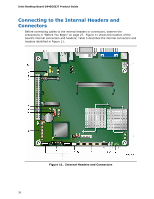
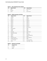
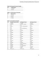
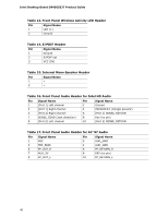
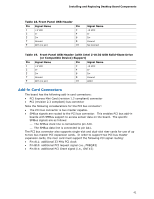
Installing and Replacing Desktop Board Components Table 18. Front Panel USB Header Pin Signal Name Pin 1 +5 VDC 2 3 D- 4 5 D+ 6 7 Ground 8 9 KEY (no pin) 10 Signal Name +5 VDC DD+ Ground No Connect Table 19. Front Panel USB Header (with Intel Z-U130 USB Solid-State Drive (or Compatible Device) Support) Pin Signal Name 1 +5 VDC 3 D- 5 D+ 7 Ground 9 KEY (no pin) Pin Signal Name 2 +5 VDC 4 D- 6 D+ 8 Ground 10 LED# Add-in Card Connectors The board has the following add-in card connectors: • PCI Express Mini Card (revision 1.2 compliant) connector • PCI (revision 2.3 compliant) bus connector Note the following considerations for the PCI bus connector: • The PCI bus connector is bus master capable. • SMBus signals are routed to the PCI bus connector. This enables PCI bus add-in boards with SMBus support to access sensor data on the board. The specific SMBus signals are as follows: ⎯ The SMBus clock line is connected to pin A40. ⎯ The SMBus data line is connected to pin A41. The PCI bus connector also supports single-slot and dual-slot riser cards for use of up to two bus master PCI expansion cards. In order to support two PCI bus master expansion cards, the riser card must support the following PCI signal routing: • Pin A11: additional 33 MHz PCI clock • Pin B10: additional PCI request signal (i.e., PREQ#2) • Pin B14: additional PCI Grant signal (i.e., GNT#2) 41
-
 1
1 -
2
-
3
-
4
-
5
-
6
-
7
-
8
-
9
-
10
-
11
-
12
-
13
-
14
-
15
-
16
-
17
-
18
-
19
-
20
-
21
-
22
-
23
-
24
-
25
-
26
-
27
-
28
-
29
-
30
-
31
-
32
-
33
-
34
-
35
-
 36
36 -
 37
37 -
 38
38 -
 39
39 -
 40
40 -
 41
41 -
 42
42 -
 43
43 -
 44
44 -
 45
45 -
 46
46 -
47
-
48
-
49
-
50
-
51
-
52
-
53
-
54
-
55
-
56
-
57
-
58
-
59
-
60
-
61
-
62
-
63
-
64
-
65
-
66
-
67
-
68
-
69
-
70
-
71
-
72
 |
 |
