Intel D34010WYK Technical Product Specification - Page 9

Regulatory Compliance and Battery Disposal Information, s, Tables - support

Page 9 highlights

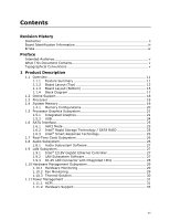
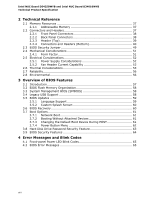
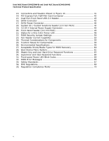
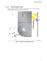
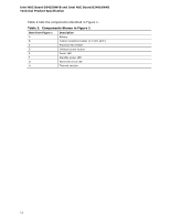
Contents 5 Regulatory Compliance and Battery Disposal Information 5.1 Regulatory Compliance 67 5.1.1 Safety Standards 67 5.1.2 European Union Declaration of Conformity Statement 68 5.1.3 EMC Regulations 69 5.1.4 e-Standby and ErP Compliance 72 5.1.5 Regulatory Compliance Marks (Board Level 73 5.2 Battery Disposal Information 74 Figures 1. Major Board Components (Top 13 2. Major Board Components (Bottom 15 3. Block Diagram 17 4. Memory Channel and SO-DIMM Configuration 20 5. 4-Pin 3.5 mm (1/8 inch) Audio Jack Pin Out 26 6. LAN Connector LED Locations 28 7. Thermal Solution and Fan Header 30 8. Location of the Standby Power LED 35 9. Front Panel Connectors 38 10. Back Panel Connectors 38 11. Header (Top 39 12. Connectors and Headers (Bottom 40 13. Connection Diagram for Front Panel Header (2.0 mm Pitch 46 14. Connection Diagram for Internal USB 2.0 Dual-Port Header (2.0 mm Pitch 48 15. Location of the CIR Sensor 48 16. Location of the BIOS Security Jumper 49 17. Board Dimensions 51 18. Localized High Temperature Zones 54 Tables 1. Feature Summary 11 2. Components Shown in Figure 1 14 3. Components Shown in Figure 2 16 4. Supported Memory Configurations 19 5. DisplayPort Multi-Streaming Resolutions 23 6. Multiple Display Configuration Maximum Resolutions 23 7. Audio Formats Supported by the Mini HDMI and Mini DisplayPort Interfaces 24 8. LAN Connector LED States 28 9. Effects of Pressing the Power Switch 31 10. Power States and Targeted System Power 32 11. Wake-up Devices and Events 33 12. Header Shown in Figure 10 39 ix

  • 1
  • 2
  • 3
  • 4
  • 5
  • 6
  • 7
  • 8
  • 9
  • 10
  • 11
  • 12
  • 13
  • 14
  • 15
  • 16
  • 17
  • 18
  • 19
  • 20
  • 21
  • 22
  • 23
  • 24
  • 25
  • 26
  • 27
  • 28
  • 29
  • 30
  • 31
  • 32
  • 33
  • 34
  • 35
  • 36
  • 37
  • 38
  • 39
  • 40
  • 41
  • 42
  • 43
  • 44
  • 45
  • 46
  • 47
  • 48
  • 49
  • 50
  • 51
  • 52
  • 53
  • 54
  • 55
  • 56
  • 57
  • 58
  • 59
  • 60
  • 61
  • 62
  • 63
  • 64
  • 65
  • 66
  • 67
  • 68
  • 69
  • 70
  • 71
  • 72
  • 73
  • 74
  • 75
  • 76
  • 77
  • 78

Contents
ix
5
Regulatory Compliance and Battery Disposal Information
5.1
Regulatory Compliance
......................................................................
67
5.1.1
Safety Standards
...................................................................
67
5.1.2
European Union Declaration of Conformity Statement
................
68
5.1.3
EMC Regulations
...................................................................
69
5.1.4
e-Standby and ErP Compliance
...............................................
72
5.1.5
Regulatory Compliance Marks (Board Level)
.............................
73
5.2
Battery Disposal Information
..............................................................
74
Figures
1.
Major Board Components (Top)
..........................................................
13
2.
Major Board Components (Bottom)
.....................................................
15
3.
Block Diagram
..................................................................................
17
4.
Memory Channel and SO-DIMM Configuration
......................................
20
5.
4-Pin 3.5 mm (1/8 inch) Audio Jack Pin Out
.........................................
26
6.
LAN Connector LED Locations
.............................................................
28
7.
Thermal Solution and Fan Header
.......................................................
30
8.
Location of the Standby Power LED
.....................................................
35
9.
Front Panel Connectors
.....................................................................
38
10. Back Panel Connectors
......................................................................
38
11. Header (Top)
...................................................................................
39
12. Connectors and Headers (Bottom)
......................................................
40
13. Connection Diagram for Front Panel Header (2.0 mm Pitch)
...................
46
14. Connection Diagram for Internal USB 2.0 Dual-Port
Header (2.0 mm Pitch)
......................................................................
48
15. Location of the CIR Sensor
................................................................
48
16. Location of the BIOS Security Jumper
.................................................
49
17. Board Dimensions
.............................................................................
51
18. Localized High Temperature Zones
.....................................................
54
Tables
1.
Feature Summary
.............................................................................
11
2.
Components Shown in Figure 1
..........................................................
14
3.
Components Shown in Figure 2
..........................................................
16
4.
Supported Memory Configurations
......................................................
19
5.
DisplayPort Multi-Streaming Resolutions
..............................................
23
6.
Multiple Display Configuration Maximum Resolutions
.............................
23
7.
Audio Formats Supported by the Mini HDMI and
Mini DisplayPort Interfaces
.................................................................
24
8.
LAN Connector LED States
.................................................................
28
9.
Effects of Pressing the Power Switch
...................................................
31
10. Power States and Targeted System Power
...........................................
32
11. Wake-up Devices and Events
.............................................................
33
12. Header Shown in Figure 10
................................................................
39