Intel D425KT Product Specification - Page 41

Signal Tables for the Connectors and Headers, Table 11., Serial Port Header

Page 41 highlights

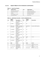
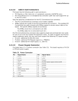
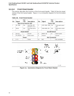
Technical Reference 2.2.2.1 Signal Tables for the Connectors and Headers Table 11. Serial Port Header Pin Signal Name 1 DCD (Data Carrier Detect) 3 TXD# (Transmit Data) 5 Ground 7 RTS (Request To Send) 9 RI (Ring Indicator) Pin 2 4 6 8 10 Signal Name RXD# (Receive Data) DTR (Data Terminal Ready) DSR (Data Set Ready) CTS (Clear To Send) Key (no pin) Table 12. LVDS Data Connector - 30-Pin (D425KTW only) Pin 1 3 5 7 9 11 13 15 17 19 21 23 25 27 29 Signal Name LA_CLKN LA_CLKP EDID_3.3V LA_DATAN0 LA_DATAP0 LA_DATAN1 LA_DATAP1 GND LA_DATAN2 LA_DATAP2 GND GND 3.3 V/5 V/12 V 3.3 V/5 V/12 V EDID_CLK Description LVDS Channel A diff clock output negative LVDS Channel A diff clock output positive Power for EDID ROM LVDS Channel A diff data output - negative LVDS Channel A diff data output - positive LVDS Channel A diff data output - negative LVDS Channel A diff data output - positive Ground LVDS Channel A diff data output - negative LVDS Channel A diff data output - positive Ground Ground Selectable LCD power output Selectable LCD power output EDID/DDC clock signal Pin 2 4 6 8 10 12 14 16 18 20 22 24 26 28 30 Signal Name NC Description NC EDID_GND NC Ground for EDID signaling NC NC NC GND NC Ground NC GND GND 3.3 V/5 V/12 V 3.3 V/5 V/12 V EDID_DATA Ground Ground Selectable LCD power output Selectable LCD power output EDID/DDC data signal 41

  • 1
  • 2
  • 3
  • 4
  • 5
  • 6
  • 7
  • 8
  • 9
  • 10
  • 11
  • 12
  • 13
  • 14
  • 15
  • 16
  • 17
  • 18
  • 19
  • 20
  • 21
  • 22
  • 23
  • 24
  • 25
  • 26
  • 27
  • 28
  • 29
  • 30
  • 31
  • 32
  • 33
  • 34
  • 35
  • 36
  • 37
  • 38
  • 39
  • 40
  • 41
  • 42
  • 43
  • 44
  • 45
  • 46
  • 47
  • 48
  • 49
  • 50
  • 51
  • 52
  • 53
  • 54
  • 55
  • 56
  • 57
  • 58
  • 59
  • 60
  • 61
  • 62
  • 63
  • 64
  • 65
  • 66
  • 67
  • 68
  • 69
  • 70
  • 71
  • 72
  • 73
  • 74
  • 75
  • 76
  • 77
  • 78
  • 79
  • 80
  • 81
  • 82
  • 83
  • 84
  • 85
  • 86
  • 87
  • 88
  • 89

Technical Reference
41
2.2.2.1
Signal Tables for the Connectors and Headers
Table 11.
Serial Port Header
Pin
Signal Name
Pin
Signal Name
1
DCD (Data Carrier Detect)
2
RXD# (Receive Data)
3
TXD# (Transmit Data)
4
DTR (Data Terminal Ready)
5
Ground
6
DSR (Data Set Ready)
7
RTS (Request To Send)
8
CTS (Clear To Send)
9
RI (Ring Indicator)
10
Key (no pin)
Table 12.
LVDS Data Connector - 30-Pin (D425KTW only)
Pin
Signal
Name
Description
Pin
Signal
Name
Description
1
LA_CLKN
LVDS Channel A diff
clock output -
negative
2
NC
3
LA_CLKP
LVDS Channel A diff
clock output -
positive
4
NC
5
EDID_3.3V
Power for EDID ROM
6
EDID_GND
Ground for EDID signaling
7
LA_DATAN0
LVDS Channel A diff
data output –
negative
8
NC
9
LA_DATAP0
LVDS Channel A diff
data output –
positive
10
NC
11
LA_DATAN1
LVDS Channel A diff
data output –
negative
12
NC
13
LA_DATAP1
LVDS Channel A diff
data output –
positive
14
NC
15
GND
Ground
16
GND
Ground
17
LA_DATAN2
LVDS Channel A diff
data output –
negative
18
NC
19
LA_DATAP2
LVDS Channel A diff
data output –
positive
20
NC
21
GND
Ground
22
GND
Ground
23
GND
Ground
24
GND
Ground
25
3.3 V/5 V/12 V
Selectable LCD
power output
26
3.3 V/5 V/12 V
Selectable LCD power
output
27
3.3 V/5 V/12 V
Selectable LCD
power output
28
3.3 V/5 V/12 V
Selectable LCD power
output
29
EDID_CLK
EDID/DDC clock
signal
30
EDID_DATA
EDID/DDC data signal