LG 32LX2D Service Manual - Page 20
VS,Hs at RF21-23
 |
View all LG 32LX2D manuals
Add to My Manuals
Save this manual to your list of manuals |
Page 20 highlights
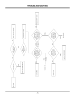
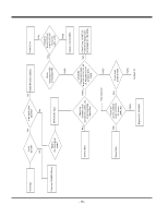
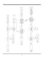
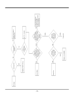
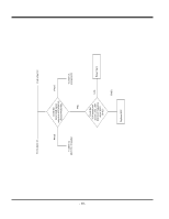
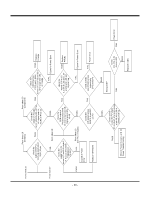
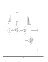
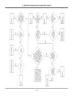
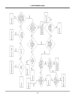
From sheet 22 From sheet 16 (S-Video) From sheet 20 (component) check the output of VSP at. 10,15,16,18,20,21,22 30,31,32 pin PASS Check the output of Froudja. at pin 148-155,130-137 for Y/C signal and clk, VS,Hs at RF21-23 FAIL check the 3.3Vdd across CF12 and 1.8Vdd across CF27,CF33 and 13.5 MHz at pin 191-192 of Froudja PASS Replace Froudja From shee 17 FAIL From sheet 18 PASS Check the supply Vcc 3.3V across L6,7 and 1.8V at pin 2 of IC11,12 and crystal Frequency at Pin 69,70 check the RGB output of PW181 across RAS 10-15 and sync and clk Signal across RS 45-48 PASS FAIL From sheet 20 (DVI PC / X-Studio) PASS Crystal or Power Error Replace VSP9437B Check the IEP output across RAIP 1-6 and RIP 1,3,4,6 FAIL FAIL FAIL Crystal or Power Error check the supply 3.3V at LS 4, 2.5V at LS3 and 1.5V at LS6 and LS9 and Crystal freq PASS Replace PW181 FAIL Crystal or Power Error check 3.3Vdd and 2.5Vdd across respectively LIP2 and LIP1 FAIL Power Error - 20 - PASS Check LVDS PASS output for PiP at pin 37,41,45,47 & for main image at pin 48,46,42,38 of IC902(LVDS IC). Check Power Levels and do Power Troubleshooting PASS Replace IEP FAIL Check Vcc_PLL 3.3V Across L901 PASS Replace LVDS Power Error FAIL
-
 1
1 -
2
-
3
-
4
-
5
-
6
-
7
-
8
-
9
-
10
-
11
-
12
-
13
-
14
-
 15
15 -
 16
16 -
 17
17 -
 18
18 -
 19
19 -
 20
20 -
 21
21 -
 22
22 -
 23
23 -
 24
24 -
 25
25 -
26
-
27
-
28
-
29
-
30
-
31
-
32
-
33
-
34
-
35
-
36
-
37
-
38
-
39
-
40
-
41
-
42
-
43
-
44
-
45
-
46
-
47
-
48
-
49
-
50
-
51
-
52
-
53
-
54
-
55
-
56
-
57
-
58
-
59
-
60
-
61
-
62
-
63
-
64
-
65
-
66
-
67
-
68
-
69
-
70
-
71
-
72
 |
 |
