MSI 790XT User Guide - Page 39
CAS Latency CL
 |
View all MSI 790XT manuals
Add to My Manuals
Save this manual to your list of manuals |
Page 39 highlights
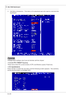
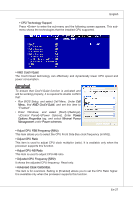
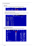
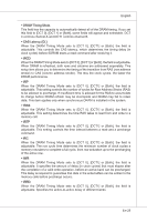
English ▶ DRAM Timing Mode This field has the capacity to automatically detect all of the DRAM timing. If you set this field to [DCT 0], [DCT 1] or [Both], some fields will appear and selectable. DCT 0 controls channel A and DCT1 controls channel B. ▶ CAS Latency (CL) When the DRAM Timing Mode sets to [DCT 0], [DCT1] or [Both], the field is adjustable. This controls the CAS latency, which determines the timing delay (in clock cycles) before SDRAM starts a read command after receiving it. ▶ tRCD When the DRAM Timing Mode sets to [DCT 0], [DCT1] or [Both], the field is adjustable. When DRAM is refreshed, both rows and columns are addressed separately. This setup item allows you to determine the timing of the transition from RAS (row address strobe) to CAS (column address strobe). The less the clock cycles, the faster the DRAM performance. ▶ tRP When the DRAM Timing Mode sets to [DCT 0], [DCT1] or [Both], the field is adjustable. This setting controls the number of cycles for Row Address Strobe (RAS) to be allowed to precharge. If insufficient time is allowed for the RAS to accumulate its charge before DRAM refresh may be incomplete and DRAM may fail to retain data. This item applies only when synchronous DRAM is installed in the system. ▶ tRAS When the DRAM Timing Mode sets to [DCT 0], [DCT1] or [Both], the field is adjustable. This setting determines the time RAS takes to read from and write to a memory cell. ▶ tRTP When the DRAM Timing Mode sets to [DCT 0], [DCT1] or [Both], the field is adjustable. This setting controls the time interval between a read and a precharge command. ▶ tRC When the DRAM Timing Mode sets to [DCT 0], [DCT1] or [Both], the field is adjustable. The row cycle time determines the minimum number of clock cycles a memory row takes to complete a full cycle, from row activation up to the precharging of the active row. ▶ tWR When the DRAM Timing Mode sets to [DCT 0], [DCT1] or [Both], the field is adjustable. It specifies the amount of delay (in clock cycles) that must elapse after the completion of a valid write operation, before an active bank can be precharged. This delay is required to guarantee that data in the write buffers can be written to the memory cells before precharge occurs. ▶ tRRD When the DRAM Timing Mode sets to [DCT 0], [DCT1] or [Both], the field is adjustable. Specifies the active-to-active delay of different banks. En-29
-
 1
1 -
2
-
3
-
4
-
5
-
6
-
7
-
8
-
9
-
10
-
11
-
12
-
13
-
14
-
15
-
16
-
17
-
18
-
19
-
20
-
21
-
22
-
23
-
24
-
25
-
26
-
27
-
28
-
29
-
30
-
31
-
32
-
33
-
 34
34 -
 35
35 -
 36
36 -
 37
37 -
 38
38 -
 39
39 -
 40
40 -
 41
41 -
 42
42 -
 43
43 -
 44
44 -
45
-
46
-
47
-
48
-
49
-
50
-
51
-
52
-
53
-
54
-
55
-
56
-
57
-
58
-
59
-
60
-
61
-
62
-
63
-
64
-
65
-
66
-
67
-
68
-
69
-
70
-
71
-
72
-
73
-
74
-
75
-
76
-
77
-
78
-
79
-
80
-
81
-
82
-
83
-
84
-
85
-
86
-
87
-
88
-
89
-
90
-
91
-
92
-
93
-
94
-
95
-
96
-
97
-
98
-
99
-
100
-
101
-
102
-
103
-
104
-
105
-
106
-
107
-
108
-
109
-
110
-
111
-
112
-
113
-
114
-
115
-
116
-
117
-
118
-
119
-
120
-
121
-
122
-
123
-
124
-
125
-
126
-
127
-
128
-
129
-
130
-
131
-
132
-
133
-
134
-
135
-
136
-
137
-
138
 |
 |