Pioneer DVL-909 Service Guide - Page 25
Pd0260a2, Pd0261a2 Cldm Assy : Ic101dvl-909 Only
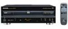 |
View all Pioneer DVL-909 manuals
Add to My Manuals
Save this manual to your list of manuals |
Page 25 highlights
DV-505, DVL-909, DV-S9 PD0260A2, PD0261A2 (CLDM ASSY : IC101)(DVL-909 ONLY) • Mechanism Control IC • Pin Function No. Pin Name 1 VCC 2 RWC 3 XPLAY 4 CLK:SCK3/CQCK 5 XCD 6 TILT ERR 7 TRK BAL ERR 8 SLD ERR 9 SLD POS 10 FSEQ 11 C DETECT 12 TRK BAL DRV 13 SHAKE 14 RF CORRECTION 15 SQOUT 16 SO3/COIN 17 SCK3/CQCK 18 SLD OUT 19 SI1 20 SO1 21 SCK 22 TRK 0 CRS 23 SBSY 24 TILT OUT 25 TURN OUT 26 XPBV 27 CNVSS 28 XRESET 29 XIN 30 XOUT I/O Function I Power supply pin Apply 5V ± 10% O DSP read/write command signal output "L"= Read "H"= Write O Signal output during spindle servo "L"= During servo "H"= During acceleration, brake and stop O DVP/DSP clock switch "H"= DVP "L"= DSP O LD/CD switch signal output "L= CD "H"= LD I A/D • This signal is A/D converted as the tilt servo control input. Control the tilt motor so that this signal becomes 2.5V. I A/D • Tracking balance error signal input This signal is A/D converted as the tracking offset control input. I A/D • This signal is A/D converted as the slider servo control input. Control the slider motor so that this signal becomes 2.5V. I A/D • Pickup position detection switch input Detect the position by reading A/D input value which each switches are resistance divided. I Subcode sync. confirmity detection signal input "L"= Not confirmity "H"= Confirmity I Spindle over-current detection signal input "L" = Over current "H"= Normal O PWM • Output the tracking offset signal to PWM output, then use for auto tracking offset. 910 µsec period, tri-state control H, L, Z I/O Handshake signal for data communication with the DVD mechanism control IC This pin is the bilateral data line and each microprocessor control the Input/Output. O RF correction switch signal output "H"= Gain UP CD, CDV-A:Low, CAV inner circuit gain up, others are High. I Command data input from DSP Read out SUBQ O Command data output to DVP/DSP O DVP/DSP read/write command clock output Read-in at rising edge O PWM • Slider control signal output 5V= FWD, 0V= REV, 2.5V= STOP 910 µsec period, tri-state control I Data input from the DVD mechanism control IC O Serial data output to the DVD mechanism control IC I/O Clock for serial communication with the DVD mechanism control IC Becomes input mode without communicate with the DVD mechanism control IC I INT • Tracking error zero cross signal input Monitor this signal when searching track count in the miss clamp detection I Subcode block sync. input I/O LOAD/TILT control output PWM output 0V : Tray IN / Tilt DOWN, 5V : Tray OUT / Tilt UP, 2.5V : STOP O Turn drive signal output I Playback vertical sync. signal input of LD/CDV "L"= During vertical sync. I Ground for A/D conversion I Reset signal input "L"= Reset "H"= Release reset Control with the DVD mechanism control IC. I 9MHz clock oscillation input O 9MHz clock oscillation output 25
-
 1
1 -
2
-
3
-
4
-
5
-
6
-
7
-
8
-
9
-
10
-
11
-
12
-
13
-
14
-
15
-
16
-
17
-
18
-
19
-
 20
20 -
 21
21 -
 22
22 -
 23
23 -
 24
24 -
 25
25 -
 26
26 -
 27
27 -
 28
28 -
 29
29 -
 30
30 -
31
-
32
-
33
-
34
-
35
-
36
-
37
-
38
-
39
-
40
-
41
-
42
-
43
-
44
-
45
-
46
-
47
 |
 |
