Sony HCD-EC68P Service Manual - Page 27
For Schematic Diagrams., For Printed Wiring Boards.
 |
View all Sony HCD-EC68P manuals
Add to My Manuals
Save this manual to your list of manuals |
Page 27 highlights
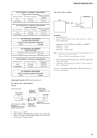
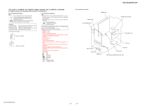
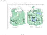
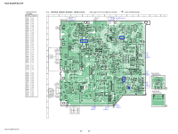
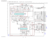
THIS NOTE IS COMMON FOR PRINTED WIRING BOARDS AND SCHEMATIC DIAGRAMS. (In addition to this, the necessary note is printed in each block.) For Printed Wiring Boards. Note: • X : Parts extracted from the component side. • Y : Parts extracted from the conductor side. • W : indicated side identified with part number. • f : Internal component. • : Pattern from the side which enables seeing. (The other layers' patterns are not indicated.) Caution: Parts face side: Parts on the parts face side seen from (Conductor Side) the pattern face are indicated. Pattern face side: Parts on the pattern face side seen from (Component Side) the parts face are indicated. • Indication of transistor. C Q These are omitted. BE Q BCE These are omitted. For Schematic Diagrams. Note: • All capacitors are in μF unless otherwise noted. (p: pF) 50 WV or less are not indicated except for electrolytics and tantalums. • All resistors are in Ω and 1/4 W or less unless otherwise specified. • f : internal component. • 2: nonflammable resistor. • C : panel designation. The components identified by mark 0 or dotted line with mark 0 are critical for safety. Replace only with part number specified. • A : B+ Line. • B : B- Line. • C : adjustment for repair. • Voltages and waveforms are dc with respect to ground under no-signal (detuned) conditions. - CD Board - no mark : CD PLAY - Other Boards - no mark : TUNER (FM/AM) • Voltages are taken with a VOM (Input impedance 10 MΩ). Voltage variations may be noted due to normal production tolerances. • Waveforms are taken with a oscilloscope. Voltage variations may be noted due to normal production tolerances. • Circled numbers refer to waveforms. • Signal path. F : FM f : AM J : CD PLAY i : AUDIO IN g : DMPORT • Abbreviation AUS : Australian model CND : Canadian model • Circuit Boards Location PANEL board KEY POWER board MAIN board HCD-EC68P/EC78P HI AMP board (EC78P) LOW AMP board KEY CD board JACK board DMP board PT board CD board REG board MOTOR board (EXCEPT EC78P: UK) HCD-EC68P/EC78P 27 27
-
 1
1 -
2
-
3
-
4
-
5
-
6
-
7
-
8
-
9
-
10
-
11
-
12
-
13
-
14
-
15
-
16
-
17
-
18
-
19
-
20
-
21
-
 22
22 -
 23
23 -
 24
24 -
 25
25 -
 26
26 -
 27
27 -
 28
28 -
 29
29 -
 30
30 -
 31
31 -
 32
32 -
33
-
34
-
35
-
36
-
37
-
38
-
39
-
40
-
41
-
42
-
43
-
44
-
45
-
46
-
47
-
48
-
49
-
50
-
51
-
52
-
53
-
54
-
55
-
56
-
57
-
58
-
59
-
60
-
61
-
62
-
63
-
64
-
65
-
66
 |
 |
